At its core, Chemical Vapor Deposition (CVD) is a sophisticated manufacturing process used to create high-performance solid materials, typically as a thin film or coating. It works by introducing a gas (a "precursor") into a chamber, which then chemically reacts or decomposes to deposit a layer of material onto a target object, known as a substrate. A prominent example is the creation of lab-grown diamonds, where carbon-rich gas deposits pure carbon onto a tiny diamond seed, growing it into a larger, flawless gem.
Chemical Vapor Deposition is not simply a coating method; it's a "bottom-up" technique for building materials atom by atom. This precision allows for the creation of exceptionally pure, uniform, and high-performance layers that are essential for modern technology, from microchips to advanced synthetic materials.
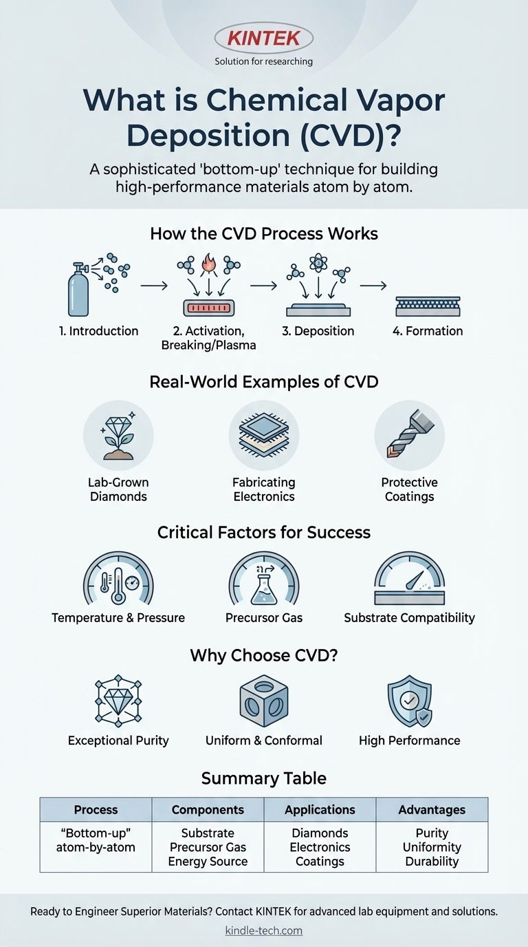
How the CVD Process Works
To truly understand CVD, it's best to break it down into its fundamental steps. The entire process takes place within a controlled vacuum chamber to ensure purity and prevent contamination.
The Key Ingredients
Every CVD process involves three primary components:
- Substrate: The object or material that will be coated. This could be a silicon wafer, a small diamond seed, or a metal tool.
- Precursor Gas: One or more volatile gases that contain the atoms of the desired deposited material. For example, a carbon-containing gas like methane is used to create diamonds.
- Energy: A source of energy, most often high heat (typically above 500°C), is used to trigger the chemical reactions.
The Step-by-Step Deposition
The process unfolds in a precise sequence.
- Introduction: The precursor gas is introduced into the vacuum chamber containing the heated substrate.
- Activation: The high temperature provides the energy to break down the gas molecules into their reactive components.
- Deposition: These individual atoms or molecules travel through the chamber and land on the surface of the substrate.
- Formation: The atoms bond to the substrate and to each other, gradually building up a solid, uniform, and highly pure film or crystal structure.
Real-World Examples of CVD in Action
While the concept might seem abstract, CVD is a foundational technology behind many high-performance products we encounter.
Example 1: Creating Lab-Grown Diamonds
This is the most well-known application. A small, thin slice of a diamond, called a seed, is placed in the chamber. The chamber is heated to around 800°C and filled with a carbon-rich gas. The gas ionizes, breaking down into pure carbon atoms that attach to the seed, growing a new diamond layer by atomic layer.
Example 2: Fabricating Electronics
CVD is indispensable in the semiconductor industry. It is used to deposit the ultra-thin, perfectly uniform films required to build microchips. These layers can be insulators (like silicon dioxide) or conductors, forming the intricate circuits that power all modern electronic devices.
Example 3: Applying Durable Protective Coatings
CVD is used to apply ultra-hard, low-friction coatings to industrial tools like drill bits and cutting blades. This significantly increases their lifespan, durability, and performance by protecting them from wear and heat.
Understanding the Trade-offs and Critical Factors
The success of the CVD process is not automatic; it relies on precise control over several critical variables. Mismanaging these can lead to poor quality deposits.
The Importance of Temperature and Pressure
The temperature must be high enough to activate the chemical reaction but not so high that it damages the substrate. The vacuum pressure must be carefully controlled to ensure the purity of the environment and manage the flow of the gas molecules.
The Role of the Precursor Gas
The choice of gas is fundamental, as it directly determines the material being deposited. The flow rate of the gas also impacts the growth rate and uniformity of the final film.
Substrate Compatibility
The substrate material must be able to withstand the high temperatures and chemical environment of the CVD process without warping or reacting undesirably. The surface of the substrate also needs to be exceptionally clean to ensure the deposited film adheres properly.
Why Is CVD the Right Choice?
Choosing a manufacturing process depends entirely on the desired outcome. CVD is selected when precision, purity, and performance are non-negotiable.
- If your primary focus is material purity and perfection: CVD is ideal because it builds materials atom-by-atom, resulting in flawless crystal structures perfect for semiconductors and high-quality diamonds.
- If your primary focus is creating thin, conformal coatings: CVD excels at depositing a film that perfectly follows the surface contours of a complex object, ensuring complete and uniform coverage.
- If your primary focus is high performance and durability: The dense, strongly-bonded materials created by CVD are exceptionally hard and resistant to wear, making them superior for protective coatings.
Ultimately, Chemical Vapor Deposition is a foundational technology that enables us to engineer materials with a level of precision that was once unimaginable.
Summary Table:
| Key Aspect | Description |
|---|---|
| Process | A "bottom-up" technique for building materials atom-by-atom in a vacuum chamber. |
| Key Components | Substrate, Precursor Gas, and an Energy Source (typically high heat). |
| Primary Applications | Lab-grown diamonds, semiconductor fabrication, ultra-hard protective coatings. |
| Main Advantages | Exceptional material purity, uniform and conformal coatings, high-performance durability. |
Ready to Engineer Superior Materials with Precision?
If your laboratory work demands the creation of high-purity thin films, flawless crystals, or durable protective coatings, the principles of CVD are critical to your success. KINTEK specializes in providing the advanced lab equipment and consumables needed to achieve these precise results.
We understand the critical factors for a successful deposition process. Let us help you select the right tools for your specific substrate and material goals.
Contact our experts today to discuss how our solutions can enhance your research and development, from semiconductor fabrication to advanced material synthesis.
Visual Guide
Related Products
- CVD Diamond Dressing Tools for Precision Applications
- Multi Heating Zones CVD Tube Furnace Machine Chemical Vapor Deposition Chamber System Equipment
- CVD Diamond Domes for Industrial and Scientific Applications
- CVD Diamond for Thermal Management Applications
- Chemical Vapor Deposition CVD Equipment System Chamber Slide PECVD Tube Furnace with Liquid Gasifier PECVD Machine
People Also Ask
- Does the chemical vapor deposition be used for diamonds? Yes, for Growing High-Purity Lab Diamonds
- How do CVD diamonds grow? A Step-by-Step Guide to Lab-Grown Diamond Creation
- How do you identify a CVD diamond? The Definitive Guide to Lab-Grown Diamond Verification
- What color diamonds are CVD? Understanding the Process from Brown Tint to Colorless Beauty
- How long does it take to make synthetic diamonds? Discover the 6-8 Week Science Behind Lab-Grown Gems


