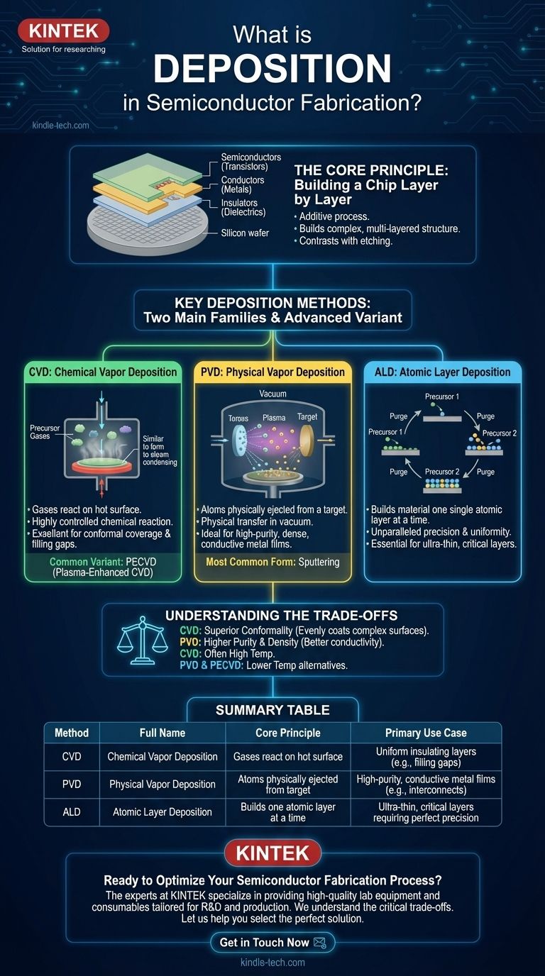
In semiconductor fabrication, deposition is the fundamental process of applying thin films of material onto a silicon wafer. This is an additive process, meaning it builds up the intricate, multi-layered structure of a microchip. It stands in direct contrast to etching, which is a subtractive process that removes material to create patterns.
Deposition is not a single action but a category of highly-controlled techniques used to construct a chip layer by atomic layer. The specific method chosen—whether chemical or physical—is a critical engineering decision that directly dictates the final performance, reliability, and cost of the semiconductor device.
The Core Principle: Building a Chip Layer by Layer
A modern microprocessor is like an incredibly complex, microscopic skyscraper with billions of components. Deposition is the process used to construct each floor and the wiring between them.
An Additive Process
Think of the silicon wafer as the foundation of the building. Deposition is the process of adding a new, perfectly uniform layer of material across that entire foundation. This could be a layer of insulation, a conductive metal, or another semiconductor material.
The Purpose of Deposited Layers
Each deposited layer serves a specific function.
- Insulators (dielectrics), like silicon dioxide (SiO₂), prevent electrical current from leaking between different components.
- Conductors, like copper or aluminum, form the "wires" or interconnects that shuttle signals around the chip.
- Semiconductors, like polysilicon, are used to build the transistors themselves—the on/off switches that are the basis of all digital logic.
Key Deposition Methods: The Two Main Families
Engineers use two primary families of techniques to deposit these layers, each with distinct advantages and use cases. The choice depends entirely on the material being deposited and the role it will play in the final device.
Chemical Vapor Deposition (CVD)
In CVD, the wafer is placed in a chamber and exposed to one or more volatile precursor gases. These gases react or decompose on the wafer's hot surface to produce the desired solid film.
This is analogous to how steam condenses into a layer of water on a cold window, but it is a highly controlled chemical reaction that creates a solid film instead of a liquid. Plasma-Enhanced CVD (PECVD) is a common variant that uses plasma to enable these reactions at lower temperatures.
Physical Vapor Deposition (PVD)
In PVD, the material to be deposited starts as a solid target. This target is bombarded with high-energy ions (typically from an argon plasma) in a vacuum, which physically dislodges atoms from the target.
These ejected atoms then travel through the vacuum and coat the wafer. The most common form of PVD is sputtering, which can be visualized as a type of atomic-scale sandblasting where the "sand" (ejected atoms) builds up to form a new layer on the wafer.
Atomic Layer Deposition (ALD)
For the most advanced applications, Atomic Layer Deposition (ALD) offers unparalleled precision. It is a type of CVD process that builds the material literally one single atomic layer at a time, providing perfect uniformity and control over thickness.
Understanding the Trade-offs
The choice between CVD and PVD is not arbitrary; it's a critical engineering trade-off based on the layer's requirements.
Conformal Coverage
CVD processes are generally superior at conformality—the ability to evenly coat complex, three-dimensional surfaces. Because the reactant gases can flow into tiny trenches and holes before reacting, they create a uniform layer, which is essential for insulating between tightly packed wires.
Purity and Density
PVD is often favored for depositing metal films because it is a physical transfer process, not a chemical one. This can result in films with higher purity and density, which leads to better electrical conductivity.
Temperature and Damage
Traditional CVD processes often require very high temperatures to drive the chemical reactions. These temperatures can damage previously fabricated layers on the chip. PVD and PECVD are valuable alternatives because they can operate at much lower temperatures.
Making the Right Choice for Your Goal
The deposition method is always chosen to serve a specific function within the chip's architecture.
- If your primary focus is creating insulating layers between metal lines: You will likely use a form of CVD (like PECVD) for its excellent ability to fill gaps and provide uniform coverage.
- If your primary focus is depositing the metal wiring (interconnects): You will likely use PVD (sputtering) to create a high-purity, dense, and highly conductive film.
- If your primary focus is building the ultra-thin, critical gate oxide of a transistor: You must use Atomic Layer Deposition (ALD) to achieve the required atomic-level precision and perfection.
Ultimately, mastering deposition is fundamental to the entire semiconductor industry, as it is the very process by which a chip is built.
Summary Table:
| Method | Full Name | Core Principle | Primary Use Case |
|---|---|---|---|
| CVD | Chemical Vapor Deposition | Gases react on a hot wafer surface to form a solid film. | Excellent for uniform insulating layers (e.g., filling gaps). |
| PVD | Physical Vapor Deposition | Atoms are physically ejected from a target to coat the wafer. | Ideal for high-purity, conductive metal films (e.g., interconnects). |
| ALD | Atomic Layer Deposition | A CVD variant that builds material one atomic layer at a time. | Essential for ultra-thin, critical layers requiring perfect precision. |
Ready to Optimize Your Semiconductor Fabrication Process?
Choosing the right deposition technique is critical for the performance and yield of your devices. The experts at KINTEK specialize in providing high-quality lab equipment and consumables tailored to the precise needs of semiconductor R&D and production.
We understand the critical trade-offs between CVD, PVD, and ALD. Let us help you select the perfect solution for your specific application, whether you are depositing insulating dielectrics or high-conductivity metal interconnects.
Contact our team today to discuss how our solutions can enhance your lab's capabilities and drive your innovations forward.
Visual Guide
Related Products
- Chemical Vapor Deposition CVD Equipment System Chamber Slide PECVD Tube Furnace with Liquid Gasifier PECVD Machine
- RF PECVD System Radio Frequency Plasma-Enhanced Chemical Vapor Deposition RF PECVD
- Customer Made Versatile CVD Tube Furnace Chemical Vapor Deposition Chamber System Equipment
- Inclined Rotary Plasma Enhanced Chemical Vapor Deposition PECVD Equipment Tube Furnace Machine
- Inclined Rotary Plasma Enhanced Chemical Vapor Deposition PECVD Equipment Tube Furnace Machine
People Also Ask
- Why is Chemical Vapor Deposition (CVD) equipment uniquely suited for constructing hierarchical superhydrophobic structures?
- What are the processes of vapor phase deposition? Understand CVD vs. PVD for Superior Thin Films
- What are the advantages of chemical vapor deposition? Achieve Superior Thin Films for Your Lab
- What is plasma enhanced chemical vapor deposition PECVD equipment? A Guide to Low-Temperature Thin Film Deposition
- What types of substrates are used in CVD to facilitate graphene films? Optimize Graphene Growth with the Right Catalyst


