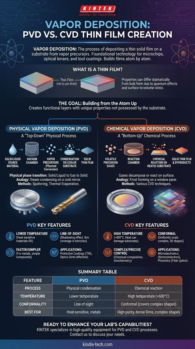
In materials science and manufacturing, the process of depositing a thin solid film on a substrate from vapor precursors is broadly known as vapor deposition. This foundational technology involves transporting material in a gaseous phase and allowing it to condense or react on a surface, building a film layer by layer. It is the core process behind the creation of microchips, advanced optical lenses, and durable tool coatings.
The central concept to grasp is that vapor deposition is not a single technique, but a family of processes divided into two main categories: Physical Vapor Deposition (PVD) and Chemical Vapor Deposition (CVD). The choice between them hinges on whether the film is formed by a physical condensation process or a chemical reaction on the substrate's surface.
The Fundamental Goal: Building from the Atom Up
At its core, vapor deposition is a form of additive manufacturing at the atomic or molecular scale. The goal is to create a functional layer with properties that the underlying substrate does not possess.
What is a "Thin Film"?
A thin film is a layer of material ranging from a few nanometers (a few dozen atoms thick) to several micrometers.
The properties of a material in a thin film can be dramatically different from its properties in bulk form due to quantum effects and surface-area-to-volume ratios.
The Role of the Substrate and Vapor
The substrate is the material or object that is being coated. It acts as the foundation upon which the film is built.
Vapor precursors are the gaseous building blocks. They are created either by turning a solid or liquid source into a gas (PVD) or by using inherently gaseous chemicals (CVD).
The Two Pillars of Vapor Deposition: PVD and CVD
Understanding the distinction between PVD and CVD is critical, as they operate on fundamentally different principles and are suited for different applications.
Physical Vapor Deposition (PVD): A "Top-Down" Physical Process
In PVD, a solid or liquid source material is physically converted into a vapor, typically inside a vacuum chamber.
This vapor then travels and condenses onto a cooler substrate, forming the solid film. It is a direct phase transition from solid/liquid to gas and back to solid.
An easy analogy is the way steam (water vapor) from a hot shower condenses into a film of liquid water on the surface of a cold mirror. Common PVD methods include sputtering and thermal evaporation.
Chemical Vapor Deposition (CVD): A "Bottom-Up" Chemical Process
In CVD, one or more volatile precursor gases are introduced into a reaction chamber.
These gases decompose or react with each other on the surface of a heated substrate, leaving behind a solid film as a byproduct of the chemical reaction.
Think of how frost forms on a window pane. Water vapor in the air doesn't just freeze onto the glass; it undergoes a phase change and crystallizes in a structured way due to the cold surface and atmospheric conditions.
Understanding the Critical Trade-offs
Neither method is universally superior. The correct choice depends entirely on the material, the substrate, and the desired outcome.
Temperature and Substrate Compatibility
CVD generally requires very high temperatures (often >600°C) to drive the necessary chemical reactions on the substrate surface. This heat can easily damage sensitive substrates like plastics or fully assembled electronic components.
PVD is a much lower-temperature process. Since it relies on condensation, it can be used to coat a far wider range of heat-sensitive materials.
Film Quality and Conformance
CVD excels at creating highly pure, dense, and conformal films. Because the precursor gases can flow around an object, CVD can uniformly coat complex, three-dimensional shapes with high precision.
PVD is fundamentally a line-of-sight process. The vaporized material travels in a straight line, which can create a "shadowing" effect and lead to thin or non-existent coverage on the backside of an object or inside deep trenches.
Process Complexity and Deposition Rate
PVD processes can sometimes be faster and mechanically simpler, especially for depositing pure metals or simple compounds.
CVD involves managing complex gas chemistries, flow rates, and high temperatures, which can increase operational costs and safety concerns. However, it offers precise control over the film's chemical composition.
Why This Process is Foundational to Modern Technology
Vapor deposition is not an obscure laboratory technique; it is a critical manufacturing step in nearly every high-tech industry.
In Microelectronics
Semiconductor fabrication is entirely dependent on vapor deposition. It is used to create the alternating layers of conducting, insulating, and semiconducting materials that form transistors and circuits on a silicon wafer.
For Protective Coatings
Hard, wear-resistant coatings, such as Titanium Nitride (TiN) on drill bits and cutting tools, are applied using PVD. This dramatically extends the tool's lifespan and performance.
In Optics and Photonics
Anti-reflective coatings on eyeglasses and camera lenses are created using PVD to deposit precise layers of materials with specific refractive indices. CVD is used to manufacture the ultra-pure glass for fiber optic cables.
Making the Right Choice for Your Goal
Selecting the correct deposition method requires matching the process capabilities to your application's primary requirement.
- If your primary focus is coating heat-sensitive materials or achieving a simple metallic layer: PVD is often the more direct and suitable choice due to its lower processing temperatures.
- If your primary focus is creating a highly pure, dense, and uniform film over a complex shape: CVD is superior for its ability to produce conformal coatings through chemical reactions.
- If your primary focus is dialing in a specific chemical composition or crystalline structure: CVD typically offers more precise control over the final film's stoichiometry and properties.
Ultimately, understanding the fundamental difference between physical condensation and chemical reaction is the key to leveraging thin-film technology for any application.
Summary Table:
| Feature | PVD (Physical Vapor Deposition) | CVD (Chemical Vapor Deposition) |
|---|---|---|
| Process | Physical condensation of vapor | Chemical reaction on substrate |
| Temperature | Lower temperature | High temperature (>600°C) |
| Coating Conformality | Line-of-sight | Conformal (covers complex shapes) |
| Best For | Heat-sensitive substrates, metals | High-purity, dense films, complex shapes |
Ready to enhance your lab's capabilities with precision thin-film deposition? KINTEK specializes in high-quality lab equipment and consumables for both PVD and CVD processes. Whether you're working with heat-sensitive materials or need conformal coatings for complex components, our solutions deliver superior performance and reliability. Contact us today to discuss how we can support your laboratory's specific thin-film deposition needs!
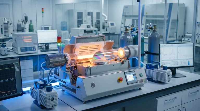
Visual Guide