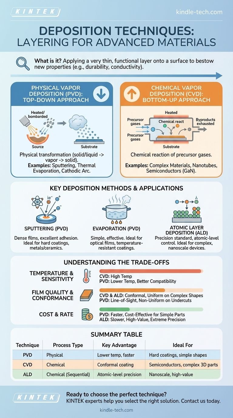
In materials science and advanced manufacturing, deposition techniques are a foundational set of processes used to apply a very thin, functional layer of one material onto the surface of another. The core purpose is to bestow new properties upon the base material—such as enhanced durability, corrosion resistance, or electrical conductivity. The most common families of these techniques are Physical Vapor Deposition (PVD) and Chemical Vapor Deposition (CVD), which accomplish this goal through fundamentally different mechanisms.
The choice of a deposition technique is not merely a procedural step; it is a strategic decision that balances the physical nature of PVD against the chemical reactivity of CVD to achieve specific film characteristics for a given application.
The Two Primary Families: PVD vs. CVD
Understanding the fundamental difference between physical and chemical deposition is the first step in navigating this landscape. The names themselves provide the most important clue.
Physical Vapor Deposition (PVD): A "Top-Down" Approach
Physical Vapor Deposition involves turning a solid or liquid source material into a vapor through purely physical means, such as heating or bombardment with ions. This vapor then travels through a vacuum and condenses onto the substrate, forming a solid thin film.
Think of it like boiling a pot of water in a cold room. The liquid water (source) turns into steam (vapor) and then condenses back into liquid water (film) on a cold window pane. The material is the same at the start and the end.
Examples of PVD methods include sputtering, thermal evaporation, and cathodic arc deposition. These are often used for depositing pure metals or simple ceramic compounds.
Chemical Vapor Deposition (CVD): A "Bottom-Up" Approach
Chemical Vapor Deposition uses volatile precursor gases that are introduced into a reaction chamber. These gases react or decompose on the heated substrate surface to form the desired thin film, with byproducts being exhausted.
This is more like mixing two clear liquids that react to form a solid precipitate. The final material is a new substance formed from the chemical combination of the starting ingredients.
CVD is essential for creating complex materials that are difficult to produce otherwise, such as carbon nanotubes or specific semiconducting layers like gallium nitride (GaN).
A Closer Look at Key Deposition Methods
While PVD and CVD are the major categories, specific techniques within them are chosen based on the desired outcome.
Sputtering (PVD)
In sputtering, a target made of the desired coating material is bombarded with high-energy ions in a vacuum. This is like a microscopic game of billiards, where the ions are cue balls that knock atoms off the target, which then travel and deposit onto the substrate.
This method is prized for creating dense films with excellent adhesion to the substrate.
Evaporation (PVD)
Evaporation is one of the simplest PVD methods. A source material is heated in a high vacuum until it evaporates, creating a vapor that travels in a straight line and coats anything in its path.
Thermal evaporation uses a resistive heat source, while electron-beam evaporation uses a focused beam of electrons to heat the material. It's highly effective for creating optical films for solar panels or temperature-resistant coatings on aerospace components.
Atomic Layer Deposition (ALD): The Precision Standard
Though not detailed in the references, it is critical to know of ALD as a distinct and increasingly important category. It is a subtype of CVD that breaks the reaction down into sequential, self-limiting steps.
This process deposits the film one single atomic layer at a time, offering unparalleled control over thickness and uniformity. It is the gold standard for coating extremely complex, 3D structures at the nanoscale.
Understanding the Trade-offs
No single technique is universally superior. The choice always involves balancing competing requirements.
Temperature and Substrate Sensitivity
CVD processes often require very high temperatures to drive the necessary chemical reactions. This can damage or warp temperature-sensitive substrates, such as plastics or certain electronic components.
PVD is generally a lower-temperature process, making it more compatible with a wider range of substrate materials.
Film Quality and Conformance
CVD and ALD excel at creating conformal coatings, meaning the film's thickness is perfectly uniform even over complex, non-flat surfaces. The precursor gases can reach every nook and cranny.
PVD is a "line-of-sight" process. The vapor travels in a straight line from the source to the substrate, making it difficult to coat undercuts or the inside of deep trenches uniformly.
Cost and Deposition Rate
Generally, PVD processes like evaporation and sputtering can deposit films much faster than CVD or ALD, making them more cost-effective for thicker coatings on simpler parts.
The extreme precision of ALD comes at the cost of a very slow deposition rate, making it suitable for high-value applications where performance is paramount.
Making the Right Choice for Your Application
Selecting the correct method requires clearly defining your project's most critical requirement.
- If your primary focus is a hard, wear-resistant coating on a simple shape (like a machining tool): PVD techniques like sputtering or cathodic arc are often the most direct and cost-effective choices.
- If your primary focus is a highly pure and uniform film on a complex semiconductor wafer: CVD is the industry standard due to its excellent conformal coverage and material versatility.
- If your primary focus is absolute precision and a pinhole-free film on a nanoscale device: ALD is the unmatched choice, justifying its slower speed and higher complexity.
- If your primary focus is a dense, temperature-resistant layer on a robust aerospace component: PVD techniques like e-beam evaporation are well-suited for this task.
Understanding these core principles moves the decision from a guess to a strategic choice based on clear engineering trade-offs.
Summary Table:
| Technique | Process Type | Key Advantage | Ideal For |
|---|---|---|---|
| PVD (Physical Vapor Deposition) | Physical | Lower temperature, faster deposition | Hard coatings, simple shapes, metals/ceramics |
| CVD (Chemical Vapor Deposition) | Chemical | Conformal coating, complex materials | Semiconductors, complex 3D parts, carbon nanotubes |
| ALD (Atomic Layer Deposition) | Chemical (Sequential) | Atomic-level precision, pinhole-free | Nanoscale devices, high-value applications |
Ready to choose the perfect deposition technique for your project?
At KINTEK, we specialize in providing advanced lab equipment and consumables for all your deposition needs. Whether you're developing wear-resistant coatings with PVD, creating complex semiconductor layers with CVD, or requiring the nanoscale precision of ALD, our experts are here to help you select the right solution.
We understand that the right equipment is critical to your success. Let us help you achieve superior film quality, improve your process efficiency, and accelerate your R&D.
Contact our experts today for a personalized consultation and discover how KINTEK can support your laboratory's innovation.
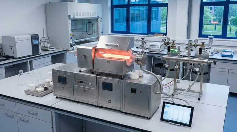
Visual Guide
Related Products
- Chemical Vapor Deposition CVD Equipment System Chamber Slide PECVD Tube Furnace with Liquid Gasifier PECVD Machine
- RF PECVD System Radio Frequency Plasma-Enhanced Chemical Vapor Deposition RF PECVD
- Inclined Rotary Plasma Enhanced Chemical Vapor Deposition PECVD Equipment Tube Furnace Machine
- Inclined Rotary Plasma Enhanced Chemical Vapor Deposition PECVD Equipment Tube Furnace Machine
- Evaporation Boat for Organic Matter
People Also Ask
- How expensive is chemical vapor deposition? Understanding the True Cost of High-Performance Coating
- What are the advantages of chemical vapor deposition? Achieve Superior Thin Films for Your Lab
- Why is Chemical Vapor Deposition (CVD) equipment uniquely suited for constructing hierarchical superhydrophobic structures?
- How are carbon nanotubes grown? Master Scalable Production with Chemical Vapor Deposition
- What happens during deposition chemistry? Building Thin Films from Gaseous Precursors


