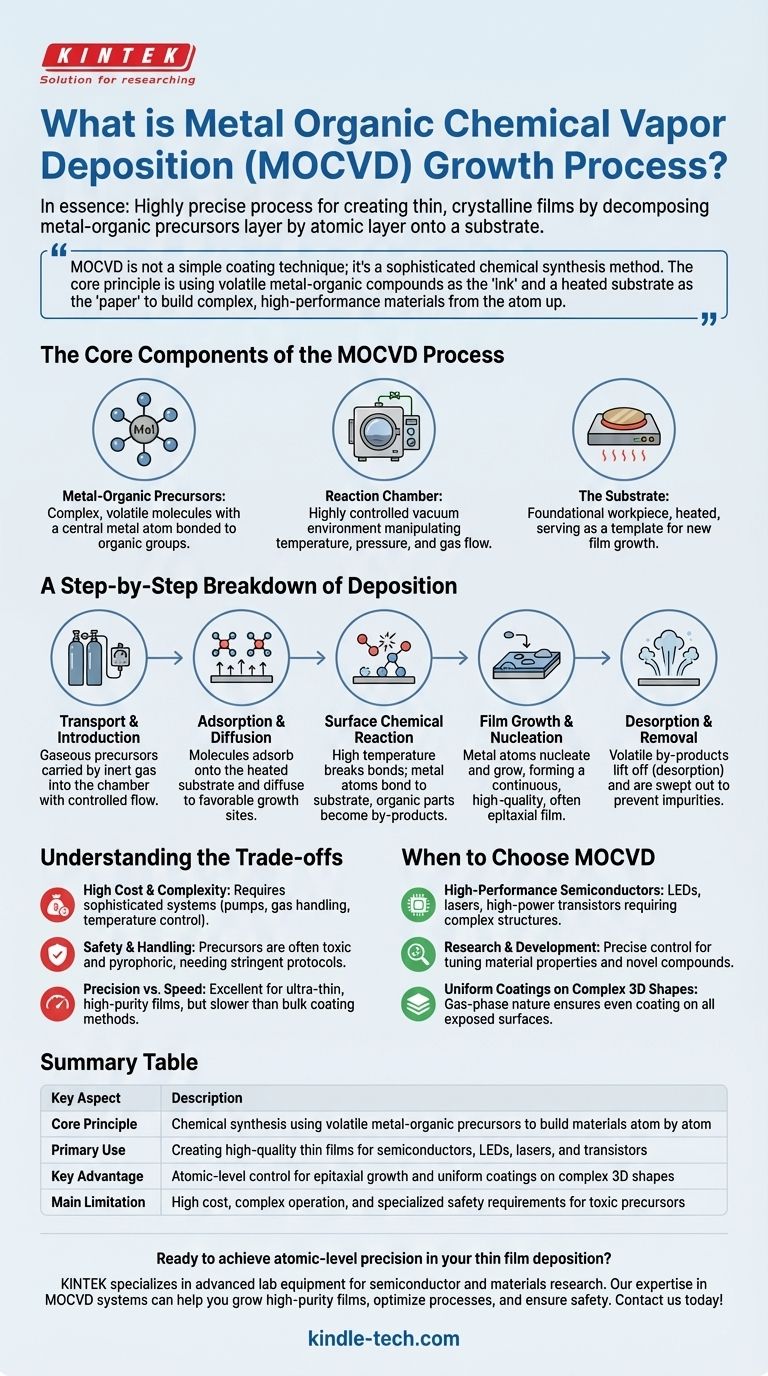
In essence, Metal-Organic Chemical Vapor Deposition (MOCVD) is a highly precise process for creating thin, crystalline films on a surface. It involves introducing specific chemical vapors, known as metal-organic precursors, into a reaction chamber where they decompose with heat and deposit a high-quality solid material, layer by atomic layer, onto a substrate.
MOCVD is not a simple coating technique; it's a sophisticated chemical synthesis method. The core principle is using volatile metal-organic compounds as the "ink" and a heated substrate as the "paper" to build complex, high-performance materials from the atom up.
The Core Components of the MOCVD Process
To understand how MOCVD works, you must first understand its three essential components. Each plays a critical and distinct role in the final outcome.
The Metal-Organic Precursors
The defining feature of MOCVD is its use of metal-organic precursors. These are complex molecules where a central metal atom is bonded to organic groups.
These molecules are engineered to be volatile, meaning they turn into a gas at relatively low temperatures without breaking down. This allows them to be transported into the reaction chamber easily.
The Reaction Chamber
This is a highly controlled environment, typically held under vacuum. The chamber allows for precise manipulation of temperature, pressure, and gas flow rates.
The substrate, which is the material to be coated, is placed inside this chamber and heated to a specific reaction temperature.
The Substrate
The substrate is the foundational workpiece upon which the new material is grown. Its own crystal structure and surface quality are critical, as they often serve as a template for the new film.
A Step-by-Step Breakdown of Deposition
The MOCVD growth process is a sequential chain of physical and chemical events that must occur in perfect order to create a high-quality film.
Transport and Introduction
The metal-organic precursors, now in a gaseous state, are carried into the reaction chamber by an inert carrier gas (like hydrogen or nitrogen). Their flow rates are meticulously controlled.
Adsorption and Diffusion
Once inside the chamber, the precursor gas molecules travel to the heated substrate and stick to its surface in a process called adsorption.
These adsorbed molecules can then diffuse, or move across the surface, to find energetically favorable locations for growth, such as an existing step in the crystal lattice.
Surface Chemical Reaction
This is the core of the process. The high temperature of the substrate provides the energy needed to break the chemical bonds within the precursor molecules.
The metal atoms detach from their organic components and bond to the substrate. The organic components are now considered by-products.
Film Growth and Nucleation
The deposited metal atoms link together, forming stable islands that nucleate and grow. Over time, these islands coalesce to form a continuous, thin film.
By carefully controlling the conditions, this growth can be epitaxial, meaning the new film's crystal structure is a perfect extension of the underlying substrate's structure.
Desorption and Removal
The volatile organic by-products that were cleaved from the precursors lift off the surface (desorption) and are swept out of the reaction chamber by the gas flow.
This continuous removal is crucial to prevent impurities from being incorporated into the growing film.
Understanding the Trade-offs
While powerful, MOCVD is a specialized technique with significant operational considerations. Understanding its limitations is key to its proper application.
High Cost and Complexity
MOCVD systems are highly complex and expensive. They require sophisticated vacuum pumps, gas handling systems for multiple precursors, and precise temperature control units.
Safety and Handling
The metal-organic precursors are often highly toxic and pyrophoric, meaning they can spontaneously ignite upon contact with air. This necessitates stringent safety protocols and specialized handling equipment.
Precision vs. Speed
MOCVD excels at creating ultra-thin, high-purity films with atomic-level control. However, it can be a relatively slow deposition process compared to other methods designed for producing thick, bulk coatings. Its strength is in quality, not quantity.
When to Choose MOCVD
The decision to use MOCVD is driven entirely by the final material requirements. It is a tool for applications where crystalline quality and compositional control are paramount.
- If your primary focus is manufacturing high-performance semiconductors: MOCVD is the industry standard for creating the complex, layered crystal structures required for LEDs, lasers, and high-power transistors.
- If your primary focus is research and development of novel materials: The precise control over gas flow and temperature makes MOCVD ideal for tuning material properties and creating experimental compounds.
- If your primary focus is achieving uniform coatings on complex 3D shapes: MOCVD's gas-phase nature ensures that all exposed surfaces are coated evenly, unlike line-of-sight physical deposition methods.
Ultimately, MOCVD is the essential tool for building the foundational materials of our modern technological world.
Summary Table:
| Key Aspect | Description |
|---|---|
| Core Principle | Chemical synthesis using volatile metal-organic precursors to build materials atom by atom |
| Primary Use | Creating high-quality thin films for semiconductors, LEDs, lasers, and transistors |
| Key Advantage | Atomic-level control for epitaxial growth and uniform coatings on complex 3D shapes |
| Main Limitation | High cost, complex operation, and specialized safety requirements for toxic precursors |
Ready to achieve atomic-level precision in your thin film deposition?
KINTEK specializes in advanced lab equipment and consumables for semiconductor and materials research. Our expertise in MOCVD systems can help you:
- Grow high-purity crystalline films with exceptional uniformity
- Optimize your deposition process for LEDs, lasers, and semiconductor devices
- Ensure safe handling of specialized precursors and gases
Let our team provide the right equipment and support for your laboratory's thin film deposition needs. Contact us today to discuss how we can enhance your research and manufacturing capabilities!
Visual Guide
Related Products
- Multi Heating Zones CVD Tube Furnace Machine Chemical Vapor Deposition Chamber System Equipment
- 915MHz MPCVD Diamond Machine Microwave Plasma Chemical Vapor Deposition System Reactor
- Microwave Plasma Chemical Vapor Deposition MPCVD Machine System Reactor for Lab and Diamond Growth
- Cylindrical Resonator MPCVD Machine System Reactor for Microwave Plasma Chemical Vapor Deposition and Lab Diamond Growth
- Molybdenum Vacuum Heat Treat Furnace
People Also Ask
- What advantages do CVD furnaces offer for Wf/W composites? Preserving Fiber Ductility and Interface Integrity
- What are the advantages of using a Multi-zone Tube Furnace? Enhanced Thermal Uniformity for Diffusion Research
- What is the function of a high-temperature CVD tube furnace in 3D graphene foam prep? Master 3D Nanomaterial Growth
- What is the function of a tube furnace in CVD SiC synthesis? Achieving Ultra-Pure Silicon Carbide Powders
- What is the synthesis and mechanism involved in the preparation of carbon nanotubes using CVD process? Master Controlled Growth for Your Application