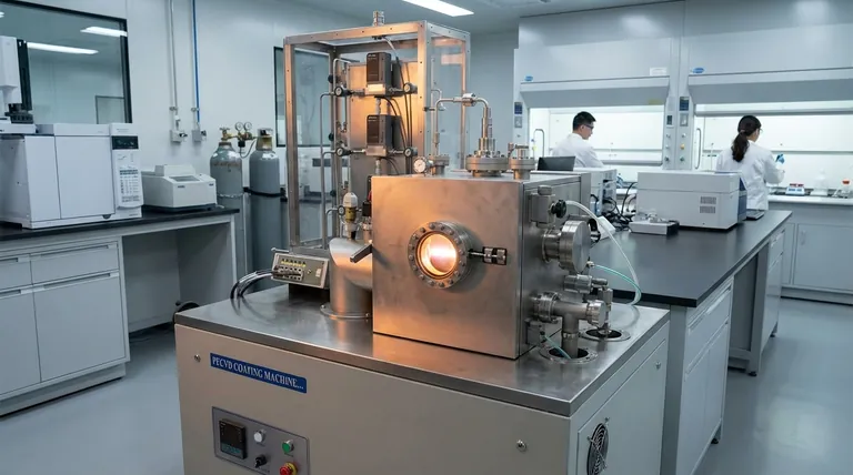
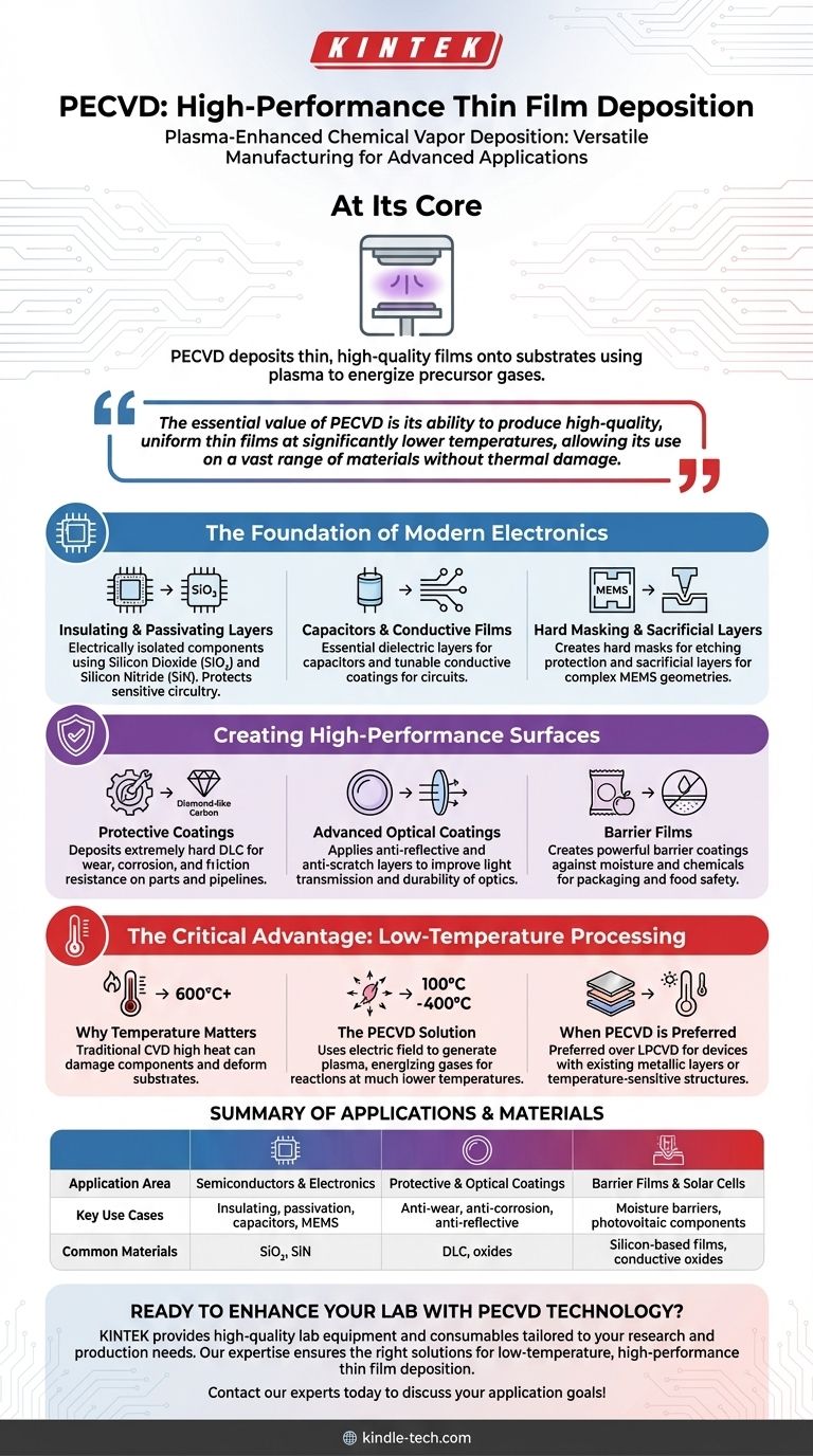
At its core, Plasma-Enhanced Chemical Vapor Deposition (PECVD) is a highly versatile manufacturing process used to deposit thin, high-performance films onto a substrate. It is a cornerstone technology in the semiconductor industry for fabricating integrated circuits, but its applications extend broadly to creating protective coatings for mechanical parts, advanced optical layers for lenses, and critical components for solar cells.
The essential value of PECVD is its ability to produce high-quality, uniform thin films at significantly lower temperatures than other methods. This low-temperature advantage allows it to be used on a vast range of materials, including those that would be damaged by intense heat, making it indispensable for modern electronics and advanced material science.
The Foundation of Modern Electronics
PECVD is a workhorse in the semiconductor and microelectronics industry. Its ability to deposit precise layers of material without high heat is crucial for building complex, multi-layered devices.
Insulating and Passivating Layers
In the fabrication of integrated circuits, components must be electrically isolated from one another. PECVD is widely used to deposit thin films of silicon dioxide (SiO₂) and silicon nitride (SiN), which act as excellent insulators and protective passivation layers that shield the sensitive circuitry.
Capacitors and Conductive Films
Beyond insulation, the process is used to create other fundamental electronic components. It can deposit the dielectric layers essential for capacitors and can also be tuned to deposit conductive coatings, forming parts of the circuit itself.
Hard Masking and Sacrificial Layers
Modern nanofabrication is a complex process of adding and removing material. PECVD is used to create hard masks, which protect specific areas during etching, and sacrificial layers, which are temporary structures used to build complex three-dimensional geometries in devices like MEMS (Micro-Electro-Mechanical Systems).
Creating High-Performance Surfaces
The benefits of PECVD extend far beyond electronics. It is a key technology for enhancing the physical properties of surfaces for industrial, optical, and consumer applications.
Protective Coatings for Durability
PECVD can deposit extremely hard and durable films, such as Diamond-like Carbon (DLC). These coatings provide exceptional wear, corrosion, and friction resistance, making them ideal for protecting mechanical parts and even large-scale infrastructure like offshore oil and gas pipelines.
Advanced Optical Coatings
In the optics industry, PECVD is used to apply anti-reflective coatings that improve light transmission through lenses and anti-scratch layers that dramatically increase the durability of eyeglasses, camera lenses, and other optical components.
Barrier Films for Packaging
The process is also used to create powerful barrier coatings against moisture and chemicals. This is especially valuable in the food and bottling industries, where thin PECVD films can protect contents and extend shelf life.
The Critical Advantage: Low-Temperature Processing
To truly understand why PECVD is so widely adopted, we must focus on its primary technical advantage over competing methods.
Why Temperature Matters
Traditional Chemical Vapor Deposition (CVD) methods require very high temperatures (often over 600°C) to trigger the chemical reactions needed to form a film. Such high heat can easily damage or destroy underlying components on a semiconductor wafer, deform plastic substrates, or alter the properties of sensitive materials.
The PECVD Solution
PECVD overcomes this limitation by introducing energy into the system using an electric field to generate a plasma. This plasma energizes the precursor gases, allowing the desired chemical reactions to occur at much lower temperatures, typically between 100°C and 400°C.
When PECVD is Preferred
Because of this, PECVD is the preferred method over Low-Pressure CVD (LPCVD) or thermal oxidation when fabricating devices with already-existing metallic layers or other temperature-sensitive structures. It opens the door to creating advanced devices that would be impossible to manufacture with high-heat processes.
Making the Right Choice for Your Goal
Selecting the right deposition technique depends entirely on the requirements of your substrate and the desired properties of your final film.
- If your primary focus is fabricating complex integrated circuits: PECVD is ideal for depositing high-quality insulating and passivation layers without damaging the delicate components already on the wafer.
- If your primary focus is enhancing the surface of a mechanical or optical part: PECVD provides a reliable method for creating durable anti-wear, anti-corrosion, or anti-reflective coatings.
- If your primary focus is working with temperature-sensitive materials: PECVD is the definitive choice over high-temperature methods, as it prevents thermal damage while still producing a high-purity, uniform film.
Ultimately, PECVD's ability to deliver high performance without the destructive cost of high heat makes it one of the most versatile and essential tools in modern manufacturing.
Summary Table:
| Application Area | Key Use Cases | Common Materials Deposited |
|---|---|---|
| Semiconductors & Electronics | Insulating layers, passivation, capacitors, MEMS | Silicon Dioxide (SiO₂), Silicon Nitride (SiN) |
| Protective & Optical Coatings | Anti-wear, anti-corrosion, anti-reflective layers | Diamond-like Carbon (DLC), various oxides |
| Barrier Films & Solar Cells | Moisture barriers, photovoltaic components | Silicon-based films, transparent conductive oxides |
Ready to enhance your lab's capabilities with PECVD technology? KINTEK specializes in providing high-quality lab equipment and consumables tailored to your research and production needs. Whether you're developing advanced semiconductors, durable coatings, or next-generation optical components, our expertise ensures you get the right solutions for low-temperature, high-performance thin film deposition. Contact our experts today to discuss how we can support your specific application goals!
Visual Guide
Related Products
- Inclined Rotary Plasma Enhanced Chemical Vapor Deposition PECVD Equipment Tube Furnace Machine
- Chemical Vapor Deposition CVD Equipment System Chamber Slide PECVD Tube Furnace with Liquid Gasifier PECVD Machine
- Inclined Rotary Plasma Enhanced Chemical Vapor Deposition PECVD Equipment Tube Furnace Machine
- RF PECVD System Radio Frequency Plasma-Enhanced Chemical Vapor Deposition RF PECVD
- Multi Heating Zones CVD Tube Furnace Machine Chemical Vapor Deposition Chamber System Equipment
People Also Ask
- What is plasma enhanced chemical vapor deposition PECVD equipment? A Guide to Low-Temperature Thin Film Deposition
- How does PECVD facilitate Ru-C nanocomposite films? Precision Low-Temperature Thin Film Synthesis
- How does PECVD equipment facilitate the directional growth of carbon nanotubes? Achieve Precision Vertical Alignment
- What are the advantages of plasma enhanced chemical vapor deposition? Enable Low-Temperature, High-Quality Film Deposition
- What are the core advantages of PE-CVD in OLED encapsulation? Protect Sensitive Layers with Low-Temp Film Deposition


