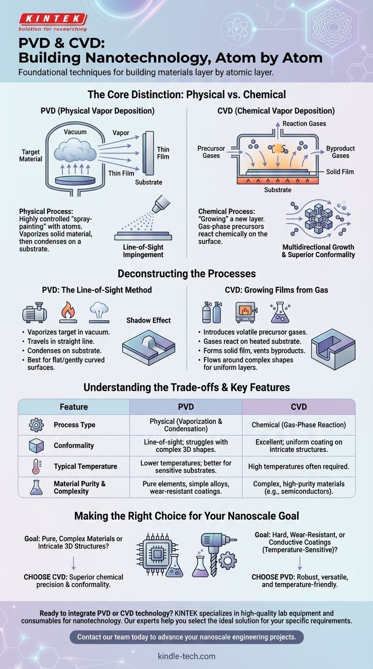
At the heart of nanotechnology is the ability to build materials layer by atomic layer. Physical Vapor Deposition (PVD) and Chemical Vapor Deposition (CVD) are two foundational techniques for achieving this. PVD is a physical process that deposits a thin film by vaporizing a solid material and having it condense on a substrate, while CVD is a chemical process that uses gas-phase precursors to react and form a solid film directly on the substrate's surface.
The core distinction is simple: PVD is like a highly controlled "spray-painting" with atoms, where a physical material travels in a line to coat a surface. CVD is more like "growing" a new layer, where gases react chemically on the surface to create a solid film from the ground up.

Deconstructing the Processes: Physical vs. Chemical
To truly grasp their roles in nanotechnology, you must understand their fundamentally different mechanisms. One is a process of transport, the other of creation.
Physical Vapor Deposition (PVD): The Line-of-Sight Method
PVD is a purely physical process where no chemical reactions occur. The process involves vaporizing a source material (the "target") inside a vacuum chamber.
This vapor then travels in a straight line and condenses on the target object, known as the substrate. Think of it as a microscopic sandblaster in reverse.
Because the vapor travels in a straight line, PVD is considered a line-of-sight impingement technique. This is highly effective for coating flat or gently curved surfaces.
Chemical Vapor Deposition (CVD): Growing Films from Gas
CVD is fundamentally a chemical process. It begins by introducing one or more volatile precursor gases into a reaction chamber, which contains the heated substrate.
These gases decompose and react on the hot substrate surface, undergoing a chemical change that forms a new, solid thin film. The byproduct gases are then vented away.
Unlike PVD, the gases in CVD can flow around complex shapes, making it a multidirectional process. This allows it to create highly uniform layers on intricate structures.
Understanding the Trade-offs
The choice between PVD and CVD is never arbitrary; it is dictated by the specific material requirements, the substrate's properties, and the desired outcome.
Conformality and Coverage
CVD's multidirectional, gas-based nature gives it superior conformality. This means it can deposit a perfectly uniform film over complex, three-dimensional nanoscale structures without shadows or thin spots.
PVD's line-of-sight nature struggles with complex geometries. Protruding features can block the vapor stream, creating "shadows" where the coating is thinner or non-existent.
Process Temperature and Substrate Compatibility
CVD often requires very high temperatures to initiate the necessary chemical reactions on the substrate's surface. This heat can damage sensitive materials, such as plastics or pre-existing electronic components.
Many PVD processes can be performed at much lower temperatures. This makes PVD suitable for a wider range of substrates that cannot withstand the thermal stress of CVD.
Material Purity and Complexity
CVD excels at creating exceptionally pure and complex materials, such as intermetallic oxides or multicomponent hybrid structures. The precision of the chemical reactions allows for fine control over the film's composition and crystal structure.
PVD is generally a more straightforward method for depositing pure elements or simple alloys. While excellent for many applications, achieving the complex stoichiometry possible with CVD is more challenging.
Making the Right Choice for Your Nanoscale Goal
Selecting the correct deposition method is critical to the success of any nanotechnology application, from nanoelectronics to protective coatings.
- If your primary focus is creating highly pure, complex semiconductor materials or uniformly coating intricate 3D structures: CVD is often the superior choice due to its chemical precision and excellent conformality.
- If your primary focus is applying a hard, wear-resistant, or conductive coating to a surface, especially one that is temperature-sensitive: PVD provides a robust, versatile, and often more direct solution.
Understanding this fundamental difference between physical deposition and chemical growth is the first step toward engineering materials at the atomic scale.
Summary Table:
| Feature | PVD (Physical Vapor Deposition) | CVD (Chemical Vapor Deposition) |
|---|---|---|
| Process Type | Physical (Vaporization & Condensation) | Chemical (Gas-Phase Reaction) |
| Conformality | Line-of-sight; struggles with complex 3D shapes | Excellent; uniform coating on intricate structures |
| Typical Temperature | Lower temperatures; better for sensitive substrates | High temperatures often required |
| Best For | Pure elements, simple alloys, wear-resistant coatings | Complex, high-purity materials (e.g., semiconductors) |
Ready to integrate PVD or CVD technology into your lab?
Choosing the right deposition method is critical for your research or production outcomes. KINTEK specializes in providing high-quality lab equipment and consumables for nanotechnology applications. Our experts can help you select the ideal PVD or CVD solution to meet your specific requirements for material purity, substrate compatibility, and coating performance.
Contact our team today to discuss how our solutions can advance your nanoscale engineering projects.
Visual Guide
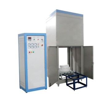
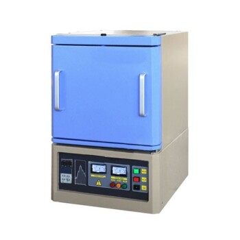
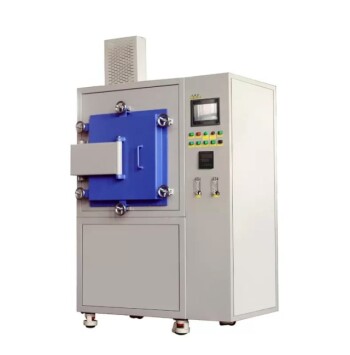
Related Products
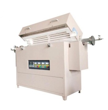
- Chemical Vapor Deposition CVD Equipment System Chamber Slide PECVD Tube Furnace with Liquid Gasifier PECVD Machine
- RF PECVD System Radio Frequency Plasma-Enhanced Chemical Vapor Deposition RF PECVD
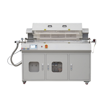
- Customer Made Versatile CVD Tube Furnace Chemical Vapor Deposition Chamber System Equipment
- Split Chamber CVD Tube Furnace with Vacuum Station Chemical Vapor Deposition System Equipment Machine
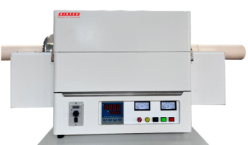
- 1200℃ Split Tube Furnace with Quartz Tube Laboratory Tubular Furnace
People Also Ask
- What is the difference between CVD and PECVD? Choose the Right Thin-Film Deposition Method
- What are the advantages of PECVD over CVD? Achieve High-Quality Thin Films at Lower Temperatures
- What is the precursor gas in PECVD? The Key to Low-Temperature Thin Film Deposition
- How are PECVD and CVD different? A Guide to Choosing the Right Thin-Film Deposition Process
- How is PECVD different from CVD? Unlock Low-Temperature Thin Film Deposition