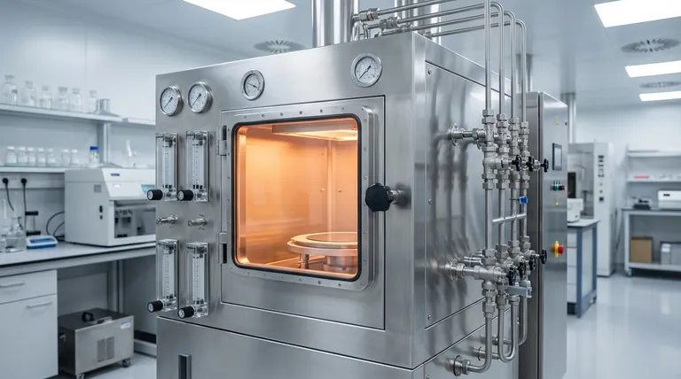
At its core, Atmospheric Pressure Chemical Vapor Deposition (APCVD) is a material science process used to create high-purity, solid thin films on a surface, known as a substrate. It works by introducing specific gases into a chamber at normal atmospheric pressure, where they react on a heated substrate to form a solid layer. This technique is fundamental to manufacturing advanced components like semiconductors and protective coatings.
The essential principle of CVD is not just coating a surface, but growing a new solid material directly onto it from a gas. The process transforms gaseous chemical precursors into a high-performance solid film through a controlled, thermally-driven reaction.
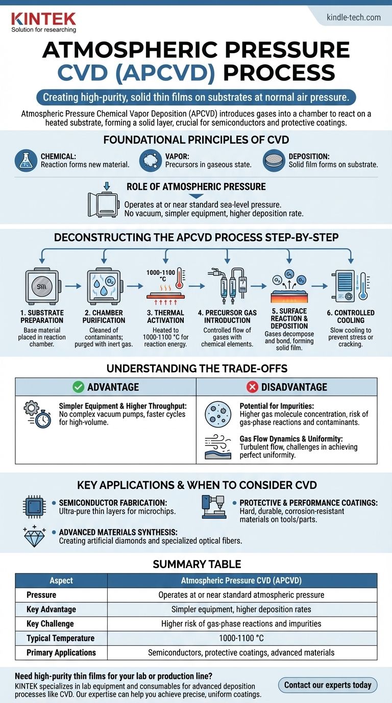
The Foundational Principles of CVD
Defining Chemical Vapor Deposition (CVD)
The name itself describes the process. Chemical refers to the chemical reaction that forms the new material. Vapor indicates that the source materials (precursors) are in a gaseous state. Deposition is the process of this new solid material forming on the substrate surface.
The Role of Atmospheric Pressure
The "Atmospheric Pressure" in APCVD specifies that the process chamber operates at or near standard sea-level air pressure. This distinguishes it from other CVD methods that require a vacuum, such as Low-Pressure CVD (LPCVD). Operating without a vacuum simplifies the equipment and can increase the deposition rate.
The Core Objective: High-Purity and Uniform Films
The ultimate goal of any CVD process is to produce films with excellent purity and uniformity across the entire substrate. This precision is why CVD is a cornerstone technology in industries like microelectronics, where even microscopic impurities can cause device failure.
Deconstructing the APCVD Process Step-by-Step
The CVD process is a carefully orchestrated sequence designed to achieve a perfect, atom-by-atom deposition of material.
1. Substrate Preparation
Everything begins with the substrate, which is the base material that will be coated (e.g., a silicon wafer or a steel tool). The substrate is placed inside the reaction chamber.
2. Chamber Purification
Before deposition can begin, the chamber must be meticulously cleaned of any contaminants. Moisture is removed, often through a thermal dehydration system, and the chamber is purged with an inert gas to eliminate residual oxygen and other impurities that could compromise the film's quality.
3. Thermal Activation
The substrate is heated to a very high temperature, often between 1000-1100 °C. This heat serves two purposes: it prepares the substrate surface for deposition and, more importantly, provides the necessary thermal energy to drive the chemical reaction.
4. Precursor Gas Introduction
With the substrate at the target temperature, precursor gases are introduced into the chamber. These gases contain the specific chemical elements that will make up the final solid film. Their flow rates are precisely controlled.
5. Surface Reaction and Deposition
When the hot precursor gases come into contact with the heated substrate, a chemical reaction occurs directly on the surface. The gases decompose, and the desired elements bond to the substrate, forming a new, solid layer that grows over time.
6. Controlled Cooling
Once the film has reached the desired thickness, the gas flow is stopped, and the system undergoes a controlled cooling process. The cooling rate is critical to prevent stress or cracking in the newly deposited film and the underlying substrate.
Understanding the Trade-offs of Atmospheric Pressure
Choosing APCVD involves a specific set of advantages and disadvantages compared to vacuum-based CVD methods.
Advantage: Simpler Equipment and Higher Throughput
Because APCVD does not require expensive and complex vacuum pumps, the reactor design is simpler and less costly. The absence of a vacuum also allows for faster processing cycles and higher deposition rates, making it suitable for high-volume manufacturing.
Disadvantage: Potential for Impurities
Operating at atmospheric pressure means there is a much higher concentration of gas molecules in the chamber. This increases the risk of unwanted gas-phase reactions and makes it more challenging to prevent airborne contaminants from being incorporated into the film.
Disadvantage: Gas Flow Dynamics and Uniformity
Gas flow at atmospheric pressure is more turbulent and less predictable than in a vacuum. This can sometimes make it more difficult to achieve perfect film thickness uniformity across large substrates, a critical factor in semiconductor fabrication.
Key Applications and When to Consider CVD
CVD is not a single solution but a versatile platform for creating advanced materials for specific, high-performance needs.
- If your primary focus is semiconductor fabrication: CVD is essential for depositing the ultra-pure, thin layers of silicon, oxides, and nitrides that form the foundation of microchips and circuit boards.
- If your primary focus is protective and performance coatings: The process is ideal for applying extremely hard, durable, and corrosion-resistant materials onto machine tools, automotive parts, and biomedical implants.
- If your primary focus is advanced materials synthesis: CVD is a key method for creating highly engineered materials that are difficult to produce otherwise, such as artificial diamonds and specialized optical fibers.
Ultimately, Chemical Vapor Deposition is a cornerstone technology that enables the creation of materials that define modern electronics and engineering.
Summary Table:
| Aspect | Atmospheric Pressure CVD (APCVD) |
|---|---|
| Pressure | Operates at or near standard atmospheric pressure |
| Key Advantage | Simpler equipment, higher deposition rates |
| Key Challenge | Higher risk of gas-phase reactions and impurities |
| Typical Temperature | 1000-1100 °C |
| Primary Applications | Semiconductors, protective coatings, advanced materials |
Need high-purity thin films for your lab or production line? KINTEK specializes in lab equipment and consumables for advanced deposition processes like CVD. Our expertise can help you achieve the precise, uniform coatings essential for semiconductors, protective layers, and advanced materials. Contact our experts today to discuss how our solutions can enhance your research and manufacturing outcomes!
Visual Guide
Related Products
- HFCVD Machine System Equipment for Drawing Die Nano-Diamond Coating
- RF PECVD System Radio Frequency Plasma-Enhanced Chemical Vapor Deposition RF PECVD
- Chemical Vapor Deposition CVD Equipment System Chamber Slide PECVD Tube Furnace with Liquid Gasifier PECVD Machine
- Customer Made Versatile CVD Tube Furnace Chemical Vapor Deposition Chamber System Equipment
- Multi Heating Zones CVD Tube Furnace Machine Chemical Vapor Deposition Chamber System Equipment
People Also Ask
- What is the specific function of the metal filament in HF-CVD? Key Roles in Diamond Growth
- What is the function of tungsten filaments in HFCVD? Powering Diamond Film Synthesis with Thermal Excitation
- What are the advantages of chemical vapor deposition? Achieve Superior Thin Films for Your Lab
- How expensive is chemical vapor deposition? Understanding the True Cost of High-Performance Coating
- What are the disadvantages and challenges of the HFCVD method? Overcome Growth Limits and Filament Issues


