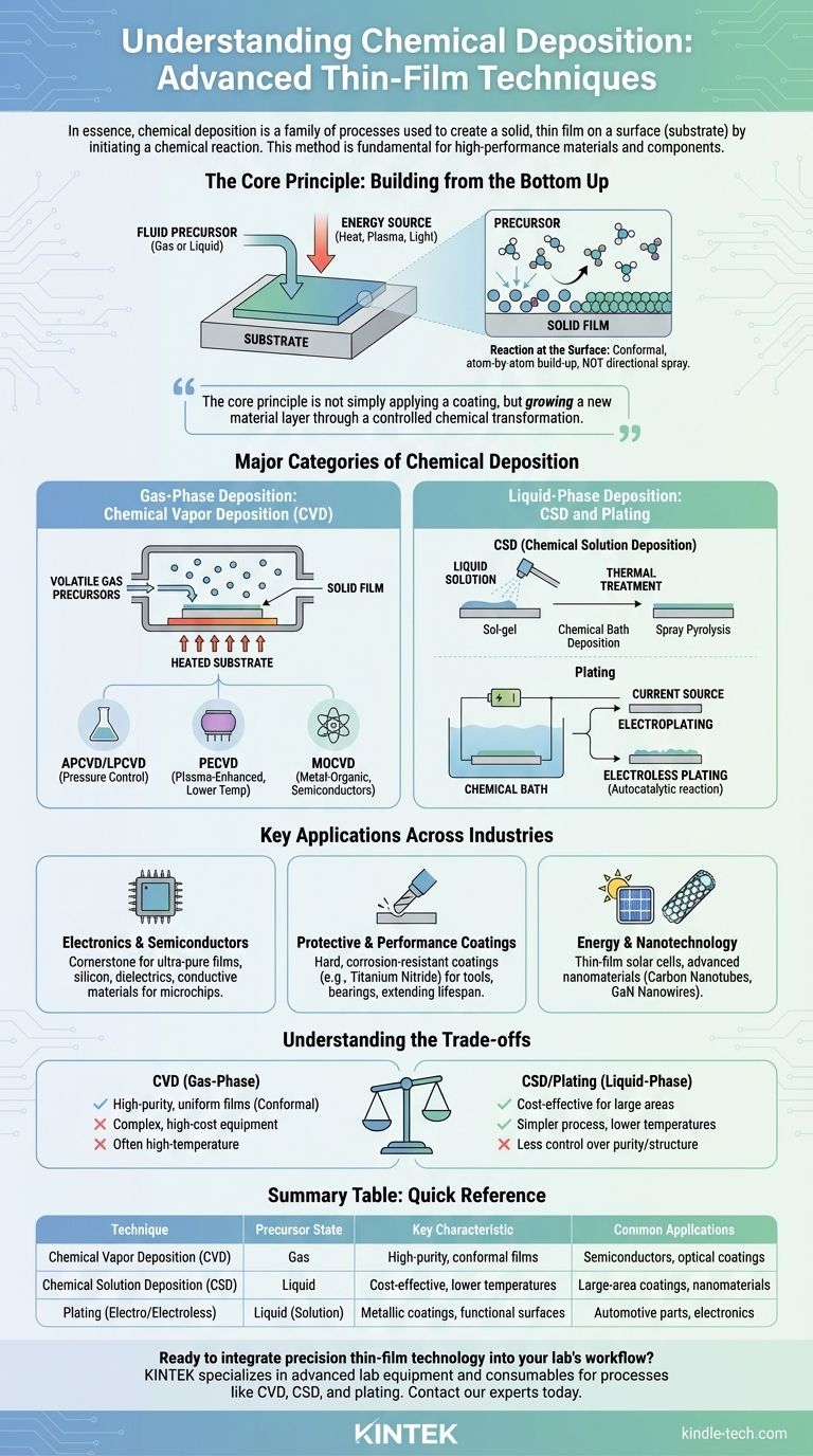
In essence, chemical deposition is a family of processes used to create a solid, thin film on a surface (known as a substrate) by initiating a chemical reaction. A fluid precursor, either a gas or a liquid, reacts at the substrate's surface, and the resulting solid product self-assembles into the desired layer. This method is fundamental to manufacturing high-performance materials and components.
The core principle of chemical deposition is not about simply applying a coating, but about growing a new material layer directly onto a surface through a controlled chemical transformation. This allows for the creation of highly uniform, pure, and complex films that conform perfectly to the underlying substrate.
The Core Principle: Building from the Bottom Up
The foundation of any chemical deposition technique is a chemical change. A precursor material, which contains the atoms for the final film, is introduced to a chamber containing the substrate.
The Reaction at the Surface
Energy is supplied to the system—often in the form of heat, plasma, or light—which causes the precursor to react or decompose. This reaction happens specifically at the solid surface, leaving behind a solid layer that builds up atom by atom or molecule by molecule.
Conformal, Not Directional
A key advantage of this method is that the films are highly conformal. Unlike processes that spray material in a straight line, the fluid precursor surrounds the substrate entirely. This means the resulting film perfectly coats all surfaces, including complex 3D shapes, trenches, and corners, with a uniform thickness.
Major Categories of Chemical Deposition
Chemical deposition isn't a single technique but a broad category defined by the state of the precursor material—either a gas or a liquid.
Gas-Phase Deposition: Chemical Vapor Deposition (CVD)
In Chemical Vapor Deposition (CVD), the precursors are volatile gases. These gases are introduced into a reaction chamber where they decompose on a heated substrate, forming the desired solid film.
CVD has many powerful variants, each optimized for different materials and applications:
- Atmospheric & Low-Pressure CVD (APCVD/LPCVD): Differ based on the chamber's operating pressure, which affects film quality and deposition rate.
- Plasma-Enhanced CVD (PECVD): Uses plasma to energize the precursor gases, allowing deposition to occur at much lower temperatures.
- Metal-Organic CVD (MOCVD): Employs metal-organic precursors, critical for manufacturing advanced semiconductors and LEDs.
Liquid-Phase Deposition: CSD and Plating
These methods use a liquid solution containing the dissolved precursors. They are often simpler and can operate at lower temperatures than CVD.
- Chemical Solution Deposition (CSD): This category includes techniques like the sol-gel process, chemical bath deposition, and spray pyrolysis. A liquid solution is applied to the substrate, followed by a thermal treatment to form the final film.
- Plating: This involves immersing the substrate in a chemical bath. In electroplating, an electric current drives the deposition of a metallic coating. In electroless plating, an autocatalytic chemical reaction deposits the film without external electricity.
Key Applications Across Industries
The precision of chemical deposition makes it essential for creating materials with specific electronic, optical, or mechanical properties.
Electronics and Semiconductors
CVD is a cornerstone of the semiconductor industry. It's used to deposit the ultra-pure, thin films of silicon, dielectrics, and conductive materials that form the basis of microchips and integrated circuits.
Protective and Performance Coatings
Hard, corrosion-resistant coatings are often applied to cutting tools, bearings, and other mechanical parts using CVD. These thin ceramic films, such as titanium nitride, dramatically extend the lifespan and performance of the underlying component.
Energy and Nanotechnology
The technique is critical for manufacturing thin-film solar cells by depositing photovoltaic materials. It is also a primary method for growing advanced nanomaterials, including carbon nanotubes and GaN nanowires, for next-generation electronics and composites.
Understanding the Trade-offs
While powerful, chemical deposition techniques require careful consideration of their complexity and cost.
Process Complexity and Control
Achieving a high-quality, uniform film requires precise control over temperature, pressure, gas flow rates, and precursor chemistry. CVD processes, in particular, often require a high level of operator skill and sophisticated, expensive equipment like vacuum systems.
Material and Temperature Limitations
The choice of technique is often dictated by the substrate's heat tolerance. High-temperature CVD can damage sensitive substrates, making lower-temperature methods like PECVD or liquid-phase deposition the only viable options.
Cost vs. Performance
Generally, gas-phase methods like CVD produce higher-purity and more uniform films but come with higher equipment and operational costs. Liquid-phase methods like CSD or plating can be more cost-effective for large-area coatings or less demanding applications but may offer less control over film purity and structure.
Making the Right Choice for Your Goal
Selecting the correct chemical deposition method depends entirely on the material requirements, substrate limitations, and production scale.
- If your primary focus is high-purity, conformal films for semiconductors or optics: A variant of Chemical Vapor Deposition (CVD) is almost always the correct choice.
- If your primary focus is cost-effective, large-area coatings or nanomaterial synthesis at lower temperatures: A Chemical Solution Deposition (CSD) method like spray pyrolysis or chemical bath is likely a better fit.
- If your primary focus is applying a functional metallic coating to a part: Electroplating or electroless plating provides a direct and well-established solution.
By understanding these techniques not just as processes but as tools for material engineering, you can precisely construct the materials required for nearly any advanced application.
Summary Table:
| Technique | Precursor State | Key Characteristic | Common Applications |
|---|---|---|---|
| Chemical Vapor Deposition (CVD) | Gas | High-purity, conformal films | Semiconductors, optical coatings |
| Chemical Solution Deposition (CSD) | Liquid | Cost-effective, lower temperatures | Large-area coatings, nanomaterials |
| Plating (Electro/Electroless) | Liquid (Solution) | Metallic coatings, functional surfaces | Automotive parts, electronics |
Ready to integrate precision thin-film technology into your lab's workflow? The right chemical deposition technique is critical for achieving the material properties your research or product demands. KINTEK specializes in providing the advanced lab equipment and consumables needed for processes like CVD, CSD, and plating. Our expertise ensures you have the reliable tools to create high-performance coatings and materials. Let's discuss your specific application – contact our experts today to find your ideal solution.
Visual Guide
Related Products
- Chemical Vapor Deposition CVD Equipment System Chamber Slide PECVD Tube Furnace with Liquid Gasifier PECVD Machine
- HFCVD Machine System Equipment for Drawing Die Nano-Diamond Coating
- 915MHz MPCVD Diamond Machine Microwave Plasma Chemical Vapor Deposition System Reactor
- RF PECVD System Radio Frequency Plasma-Enhanced Chemical Vapor Deposition RF PECVD
- Microwave Plasma Chemical Vapor Deposition MPCVD Machine System Reactor for Lab and Diamond Growth
People Also Ask
- What are the core advantages of PE-CVD in OLED encapsulation? Protect Sensitive Layers with Low-Temp Film Deposition
- How are carbon nanotubes grown? Master Scalable Production with Chemical Vapor Deposition
- What is the chemical vapor deposition growth process? Build Superior Thin Films from the Atom Up
- What types of substrates are used in CVD to facilitate graphene films? Optimize Graphene Growth with the Right Catalyst
- How expensive is chemical vapor deposition? Understanding the True Cost of High-Performance Coating