In essence, Chemical Vapor Deposition (CVD) is a manufacturing process that builds a high-purity, solid thin film on a surface using a chemical reaction from a vapor or gas. Unlike physical methods that simply transfer material, CVD creates the film through a fundamental chemical transformation of precursor gases directly onto a substrate, offering exceptional control over the material's properties.
The core principle of CVD is not to move existing solid material, but to create new solid material directly on a surface through controlled chemical reactions. This distinction is what makes it a cornerstone technology for advanced electronics and materials science.

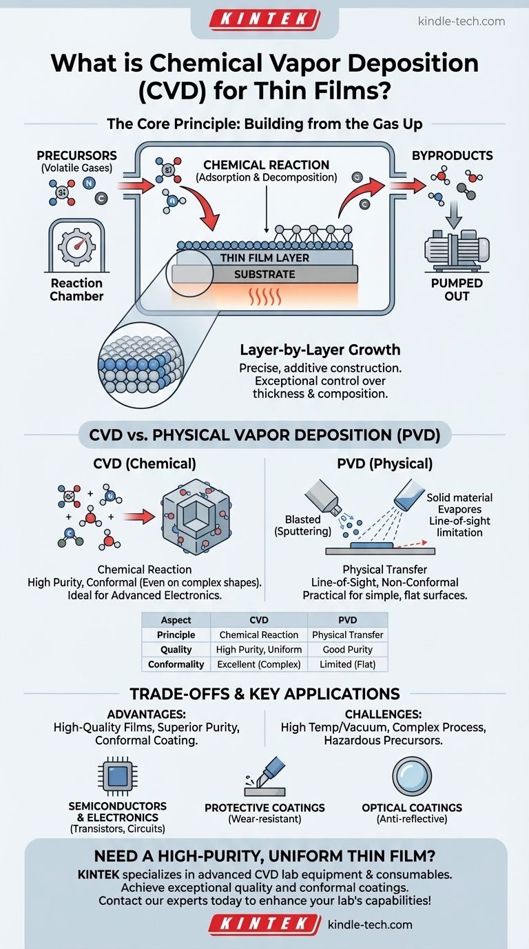
The Core Principle of CVD: Building from the Gas Up
Chemical Vapor Deposition is best understood as a precise, additive construction process happening at a microscopic scale. The entire method is based on a controlled sequence of events inside a reaction chamber.
Introducing the Precursors
The process begins with one or more volatile gases known as precursors. These gases contain the specific atoms (like silicon, nitrogen, or carbon) required for the final thin film. These precursors are carefully injected into a deposition chamber.
The Reaction on the Substrate
Inside the chamber, the target object, known as the substrate, is heated. When the precursor gases flow over this hot surface, they decompose and undergo a chemical reaction. This is the critical step of adsorption, where molecules from the gas stick to the substrate's surface.
Layer-by-Layer Growth
The chemical reaction on the surface produces the desired solid material, which deposits onto the substrate, forming a new, thin layer. Unwanted gaseous byproducts from the reaction are simply pumped out of the chamber. This process is repeated to build the film layer by layer, allowing for extremely precise control over its thickness and composition.
How CVD Differs from Physical Deposition
The most common point of confusion is the difference between chemical and physical deposition methods. The distinction is fundamental to understanding why CVD is chosen for specific applications.
Chemical Reaction vs. Physical Transfer
The defining characteristic of CVD is the chemical reaction that forms the film. In contrast, Physical Vapor Deposition (PVD) techniques involve the physical transfer of atoms from a solid source to the substrate without a chemical change.
Example: Sputtering and Evaporation (PVD)
Common PVD methods include sputtering and evaporation. Sputtering is like microscopic sandblasting, where ions are used to knock atoms off a solid target, which then coat the substrate. Evaporation involves heating a material until it turns into a gas, which then condenses on the cooler substrate. Both are line-of-sight, physical transfer processes.
The Consequence: Film Quality and Purity
Because CVD builds the film via a chemical reaction, it can produce materials of exceptionally high purity and uniformity. It also excels at creating conformal coatings, meaning it can evenly coat complex, non-flat surfaces, which is a significant challenge for line-of-sight PVD methods.
Understanding the Trade-offs
No single technique is perfect for every situation. Choosing CVD involves weighing its powerful advantages against its operational requirements.
The Advantage: High-Quality Films
CVD is the preferred method when the final film's quality is paramount. It delivers superior purity, excellent structural integrity, and the unmatched ability to uniformly coat intricate three-dimensional structures, which is essential in modern microelectronics.
The Disadvantage: Complexity and Conditions
The primary drawbacks of CVD are its process conditions. It often requires high temperatures and vacuum environments, which increases equipment cost and complexity. Furthermore, the precursor chemicals can be expensive, toxic, or hazardous, requiring strict safety protocols.
Why This Process Matters: Key Applications
The unique properties of films produced by CVD make it an indispensable technology across numerous high-tech industries.
In Semiconductors and Electronics
CVD is fundamental to manufacturing the computer chips in every modern device. It's used to deposit the thin layers of silicon, silicon dioxide (insulator), and other materials that form transistors and circuits.
For Protective and Optical Coatings
The dense, uniform layers created by CVD are ideal for producing hard, wear-resistant coatings on cutting tools and industrial equipment. It's also used to create anti-reflective optical coatings on lenses and thermal barrier coatings in the aerospace industry.
Making the Right Choice for Your Goal
Selecting a deposition method depends entirely on the requirements of the final product.
- If your primary focus is maximum purity and coating a complex shape: CVD is almost always the superior choice, as its chemical reaction-based approach ensures uniform, conformal coverage.
- If your primary focus is cost-effective coating of a simple, flat surface: A Physical Vapor Deposition (PVD) method like sputtering may be a more practical and faster alternative.
Ultimately, Chemical Vapor Deposition is the foundational process for creating the high-performance, atomically precise materials that drive modern technology.
Summary Table:
| Aspect | CVD (Chemical Vapor Deposition) | PVD (Physical Vapor Deposition) |
|---|---|---|
| Core Principle | Chemical reaction from gas precursors | Physical transfer of material (e.g., sputtering) |
| Film Quality | High purity, excellent uniformity | Good purity, can be line-of-sight limited |
| Coating Conformality | Excellent for complex, 3D surfaces | Limited for non-flat, intricate shapes |
| Typical Applications | Semiconductors, wear-resistant coatings | Simple flat surface coatings, metallization |
Need a high-purity, uniform thin film for your complex components?
KINTEK specializes in advanced lab equipment and consumables for precise Chemical Vapor Deposition processes. Our solutions help you achieve exceptional film quality, conformal coatings on intricate shapes, and reliable performance for your semiconductor, optical, or protective coating applications.
Contact our experts today to discuss how our CVD expertise can enhance your laboratory's capabilities and drive your research forward.
Visual Guide
Related Products
- Chemical Vapor Deposition CVD Equipment System Chamber Slide PECVD Tube Furnace with Liquid Gasifier PECVD Machine
- Customer Made Versatile CVD Tube Furnace Chemical Vapor Deposition Chamber System Equipment
- HFCVD Machine System Equipment for Drawing Die Nano-Diamond Coating
- Split Chamber CVD Tube Furnace with Vacuum Station Chemical Vapor Deposition System Equipment Machine
- Multi Heating Zones CVD Tube Furnace Machine Chemical Vapor Deposition Chamber System Equipment
People Also Ask
- How are carbon nanotubes grown? Master Scalable Production with Chemical Vapor Deposition
- What types of substrates are used in CVD to facilitate graphene films? Optimize Graphene Growth with the Right Catalyst
- What are the core advantages of PE-CVD in OLED encapsulation? Protect Sensitive Layers with Low-Temp Film Deposition
- What are the advantages of chemical vapor deposition? Achieve Superior Thin Films for Your Lab
- What happens during deposition chemistry? Building Thin Films from Gaseous Precursors


