The fundamental difference between vertical and horizontal furnaces in semiconductor manufacturing is the orientation of the wafers during processing. Horizontal furnaces process wafers standing vertically in a horizontal tube, while vertical furnaces process wafers lying flat in a vertical tube. This seemingly simple change in orientation has profound consequences for contamination control, process uniformity, and the ability to manufacture modern, large-diameter silicon wafers.
The industry-wide shift from horizontal to vertical furnaces was not a matter of preference, but a necessary evolution. It was driven by the relentless demand for higher device yields and tighter process control, which horizontal designs could no longer provide for larger wafers.
The Core Difference: Wafer Orientation
At the heart of semiconductor fabrication are thermal processes like oxidation, diffusion, and annealing, which require heating wafers to extreme temperatures. The furnace is the chamber where this occurs, and its design directly impacts the quality of the result.
Horizontal Furnaces: The Traditional Approach
In a horizontal furnace, wafers are loaded into a quartz "boat," standing on their edges like plates in a drying rack. This entire boat is then pushed mechanically into a long, horizontal quartz tube.
This design was the standard for decades, particularly for smaller wafers (150mm and below). It is mechanically simpler and has a lower vertical profile, fitting easily into older fabrication facilities.
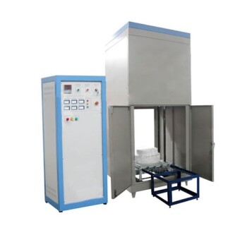
Vertical Furnaces: The Modern Standard
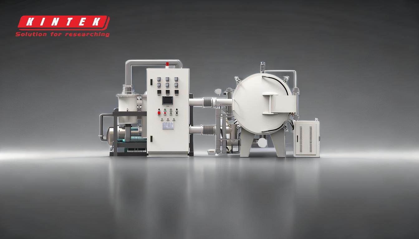
In a vertical furnace, wafers are loaded lying flat, stacked horizontally in a boat. This boat is then lowered by an elevator from the bottom or top into a vertical processing tube.
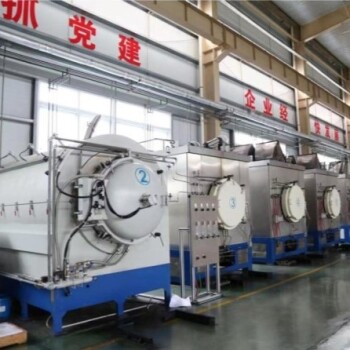
This design is dominant in all modern fabs, especially for 200mm and 300mm wafers. The entire system is taller and often requires a more complex cleanroom layout to accommodate the loading mechanics.
Why Vertical Furnaces Became the Standard
The move to vertical furnaces was a direct response to the limitations of the horizontal design, which became critical as wafer sizes increased and device features shrank.
Superior Particle Control
In a horizontal furnace, any particles that fall from the top of the tube land directly on the active surface of the wafers below. This is a major source of yield-killing defects.
Vertical furnaces solve this with gravity. Particles fall downwards, parallel to the flat surface of the wafers. Most contaminants land only on the topmost wafer in the stack, which is often a sacrificial or "dummy" wafer, protecting the valuable product wafers beneath it.
Unmatched Thermal Uniformity
Achieving a perfectly uniform temperature across every wafer is critical for consistent film growth and device performance. Horizontal furnaces struggle with this due to natural convection. Hot gas rises, creating a temperature gradient from the top to the bottom of the tube.
In a vertical furnace, the symmetrical, circular heating elements and vertical gas flow create a highly stable and radially uniform temperature zone. This ensures every wafer in the stack, and the entire surface of each wafer, experiences the exact same thermal conditions, leading to superior oxide uniformity.
Enhanced Wafer Support for Large Diameters
As wafers grew larger and thinner, physical stability became a concern. Standing a large 300mm wafer on its edge at over 1000°C, as a horizontal furnace requires, introduces stress and can cause warping.
Laying the wafer flat in a vertical furnace provides uniform support across its entire surface, preventing gravity-induced stress and deformation. This is essential for maintaining the perfect flatness required for subsequent photolithography steps.
Understanding the Trade-offs
While vertical furnaces offer superior performance, the choice is not without considerations. Horizontal furnaces still exist for specific applications due to their own set of advantages.
Footprint and Facility Cost
Vertical furnaces are tall and require significant vertical cleanroom space, often extending into the sub-fab level below. This increases facility construction costs and complexity.
Horizontal furnaces, by contrast, are long but have a low vertical profile, making them easier to install in facilities not designed for tall equipment.
Cost and Complexity
The robotic systems for loading and unloading vertical furnaces are more complex than the simple push-rod mechanisms of horizontal systems. This can translate to a higher initial capital investment and potentially more complex maintenance routines.
For processes where the ultimate level of control is not required, a horizontal furnace can be a more cost-effective solution.
Making the Right Choice for Your Goal
The choice between furnace types is ultimately dictated by the technical requirements of the process and the size of the wafer.
- If your primary focus is leading-edge manufacturing (200mm/300mm wafers): The vertical furnace is the only choice, as its superior contamination control and thermal uniformity are non-negotiable for achieving high yields.
- If your primary focus is on legacy products, R&D, or non-critical layers on smaller wafers: A horizontal furnace can be a perfectly viable and cost-effective tool that simplifies facility requirements.
Ultimately, understanding the physics of contamination and heat flow within these systems reveals why the industry evolved, prioritizing process control above all else.
Summary Table:
| Feature | Horizontal Furnace | Vertical Furnace |
|---|---|---|
| Wafer Orientation | Wafers stand vertically | Wafers lie flat |
| Particle Control | Particles fall onto wafer surfaces | Gravity pulls particles away from wafers |
| Thermal Uniformity | Challenged by convection | Superior radial and wafer-to-wafer uniformity |
| Ideal Wafer Size | Legacy, R&D, smaller wafers (≤150mm) | Modern manufacturing (200mm/300mm) |
| Footprint | Long, low vertical profile | Tall, requires vertical cleanroom space |
Ready to Optimize Your Semiconductor Thermal Processing?
Choosing the right furnace technology is critical for achieving high yields and process uniformity. KINTEK specializes in providing advanced laboratory equipment and consumables, including solutions for semiconductor thermal processing. Our expertise can help you select the ideal furnace configuration for your specific wafer size and process requirements.
Contact us today to discuss how our solutions can enhance your lab's efficiency and drive your semiconductor manufacturing forward. Get in touch via our contact form to speak with an expert.
Related Products
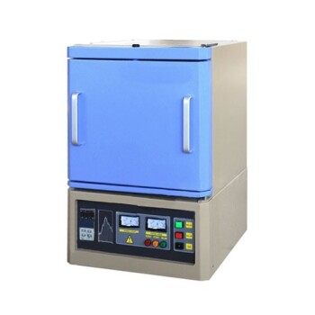
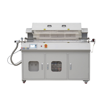
- Customer Made Versatile CVD Tube Furnace Chemical Vapor Deposition Chamber System Equipment
- 1700℃ Laboratory Quartz Tube Furnace with Alumina Tube Tubular Furnace
- 1400℃ Laboratory Quartz Tube Furnace with Alumina Tube Tubular Furnace
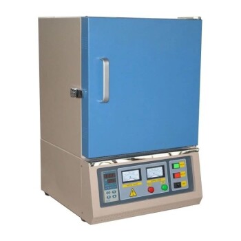
- Vertical Laboratory Quartz Tube Furnace Tubular Furnace
- Split Chamber CVD Tube Furnace with Vacuum Station Chemical Vapor Deposition System Equipment Machine
People Also Ask
- What makes nanotubes special? Discover the Revolutionary Material Combining Strength, Conductivity & Lightness
- What makes carbon nanotubes unique? Unlocking Superior Performance in Batteries & Composites
- Can carbon nanotubes form naturally? Yes, and here's where nature makes them.
- How does chemical vapor deposition work for carbon nanotubes? A Guide to Controlled Synthesis
- Why don't we use carbon nanotubes? Unlocking the Potential of a Supermaterial