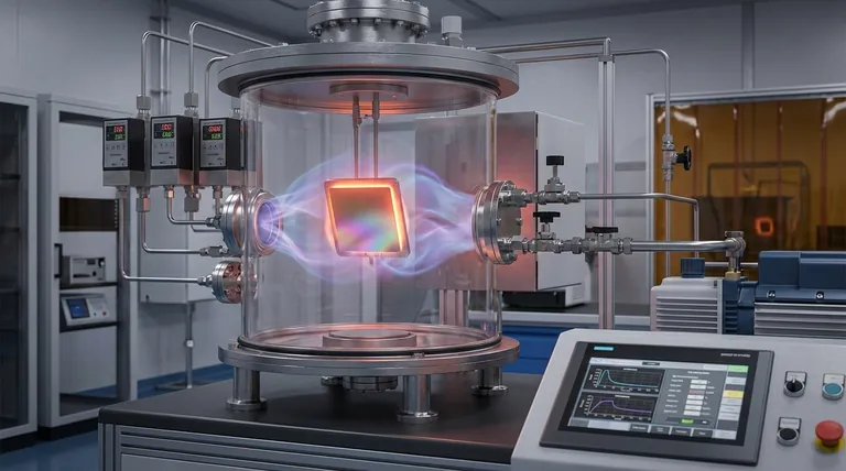
In essence, chemical vapor deposition (CVD) is a manufacturing process that builds a solid, high-performance film on a surface from a chemical reaction in a gaseous state. A workpiece, or substrate, is placed in a vacuum chamber and heated, then exposed to volatile precursor gases. These gases react and decompose on the hot surface, leaving behind a thin, exceptionally pure, and uniform layer of the desired material.
The fundamental challenge in advanced materials is depositing a perfectly uniform, high-purity thin film onto a substrate, especially on complex shapes. Chemical vapor deposition solves this by using a gas to "paint" a surface atom-by-atom, transforming a volatile precursor into a solid coating through a controlled chemical reaction.
The Core Principles of CVD
To truly understand the process, you must see it not as a simple coating method, but as a carefully controlled chemical synthesis occurring directly on a component's surface. Three elements are critical: the precursor, the vacuum, and the heat.
The Role of the Precursor Gas
The precursor is a volatile chemical compound that contains the atoms you wish to deposit. Think of it as the "ink" for this atomic-level printing process.
This gas is injected into the reaction chamber, where it flows around the substrate. The choice of precursor is critical as it dictates the final film's composition, purity, and properties.
The Importance of the Vacuum Chamber
The entire process takes place inside a vacuum chamber for two key reasons. First, it removes air and other potential contaminants that could interfere with the chemical reaction and become impurities in the final film.
Second, controlling the pressure allows for precise management of the gas flow and reaction kinetics, ensuring the process is stable and repeatable.
The Function of Heat
Heat is the catalyst for the entire process. The substrate is heated to a specific reaction temperature, often several hundred degrees Celsius.
This thermal energy provides the activation energy needed for the precursor gases to either decompose (break down) or react with other gases right at the substrate's surface. This surface-specific reaction is what ensures the film grows on the part, not elsewhere in the chamber.
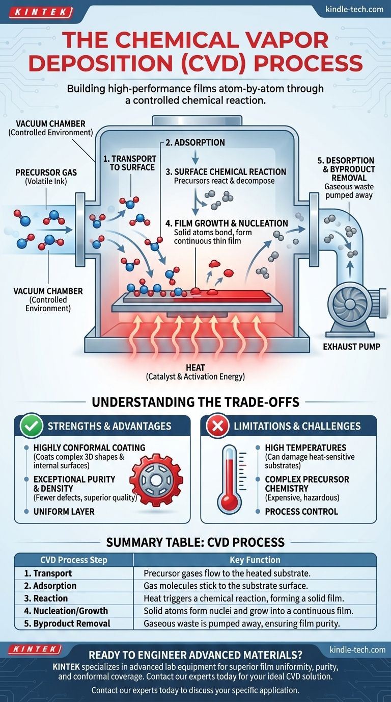
A Step-by-Step Breakdown of the Deposition Process
While the concept is straightforward, the physical process occurs in several distinct microscopic stages.
1. Transport to the Surface
Volatile precursor gases are transported into the chamber and flow towards the heated substrate. The pressure and flow rates are precisely controlled to ensure a steady supply of reactants to the surface.
2. Adsorption on the Surface
Once at the substrate, the precursor gas molecules physically stick to the hot surface in a process called adsorption. They are now held in place, ready for the main event.
3. Surface Chemical Reaction
With the molecules adsorbed on the surface, the high temperature provides the energy needed for the chemical reaction to occur. Precursors break apart and react, forming the desired solid material and other gaseous byproducts.
4. Film Growth and Nucleation
The newly formed solid atoms bond to the substrate and to each other. They begin to form tiny islands, or nuclei, which then grow and merge together to create a continuous, uniform thin film across the entire surface.
5. Desorption and Removal of Byproducts
The unwanted gaseous byproducts from the chemical reaction detach from the surface (desorption) and are removed from the chamber by the vacuum pump system. This continuous removal is crucial to maintain the reaction's efficiency and the film's purity.
Understanding the Trade-offs
CVD is a powerful technique, but its application involves important trade-offs that must be considered.
High Temperatures Can Be a Limitation
The high temperatures required for many CVD processes are its most significant drawback. This can damage or fundamentally alter heat-sensitive substrates, such as plastics or certain electronic components, making the process unsuitable for those applications.
Precursor Chemistry is Complex
The performance of CVD is entirely dependent on the precursor chemicals used. These can be expensive, hazardous, or difficult to handle. Developing the right precursor chemistry for a new material is a significant scientific challenge.
Conformal Coating is a Major Strength
A key advantage of CVD is its ability to produce highly conformal coatings. Because the precursor is a gas, it can penetrate and coat complex 3D shapes, sharp corners, and even the internal surfaces of a part with exceptional uniformity. This is something line-of-sight physical deposition methods cannot do.
Making the Right Choice for Your Goal
Selecting a deposition method depends entirely on the requirements of your final product.
- If your primary focus is coating complex 3D shapes or internal surfaces: CVD is often the superior choice due to its ability to create highly conformal films.
- If your primary focus is achieving the highest film purity and density: The chemical reaction process of CVD typically results in films with fewer defects and superior structural quality.
- If your primary focus is working with heat-sensitive materials: You must consider lower-temperature CVD variants (like Plasma-Enhanced CVD) or explore alternative methods like Physical Vapor Deposition (PVD).
By understanding CVD as a controlled chemical reaction, you can effectively leverage its power to engineer and create advanced materials with precision.
Summary Table:
| CVD Process Step | Key Function |
|---|---|
| 1. Transport | Precursor gases flow to the heated substrate. |
| 2. Adsorption | Gas molecules stick to the substrate surface. |
| 3. Reaction | Heat triggers a chemical reaction, forming a solid film. |
| 4. Nucleation/Growth | Solid atoms form nuclei and grow into a continuous film. |
| 5. Byproduct Removal | Gaseous waste is pumped away, ensuring film purity. |
Ready to Engineer Advanced Materials with Precision?
Chemical vapor deposition is key to creating high-performance coatings for semiconductors, cutting tools, and aerospace components. KINTEK specializes in providing the advanced lab equipment and consumables you need to master CVD and other thin-film processes.
Our expertise helps you achieve superior film uniformity, purity, and conformal coverage on even the most complex geometries.
Contact our experts today to discuss your specific application and discover the ideal CVD solution for your laboratory's challenges.
Visual Guide
Related Products
- Chemical Vapor Deposition CVD Equipment System Chamber Slide PECVD Tube Furnace with Liquid Gasifier PECVD Machine
- RF PECVD System Radio Frequency Plasma-Enhanced Chemical Vapor Deposition RF PECVD
- Microwave Plasma Chemical Vapor Deposition MPCVD Machine System Reactor for Lab and Diamond Growth
- Customer Made Versatile CVD Tube Furnace Chemical Vapor Deposition Chamber System Equipment
- 915MHz MPCVD Diamond Machine Microwave Plasma Chemical Vapor Deposition System Reactor
People Also Ask
- How expensive is chemical vapor deposition? Understanding the True Cost of High-Performance Coating
- Why is Chemical Vapor Deposition (CVD) equipment uniquely suited for constructing hierarchical superhydrophobic structures?
- How are carbon nanotubes grown? Master Scalable Production with Chemical Vapor Deposition
- What are the processes of vapor phase deposition? Understand CVD vs. PVD for Superior Thin Films
- What are the core advantages of PE-CVD in OLED encapsulation? Protect Sensitive Layers with Low-Temp Film Deposition


