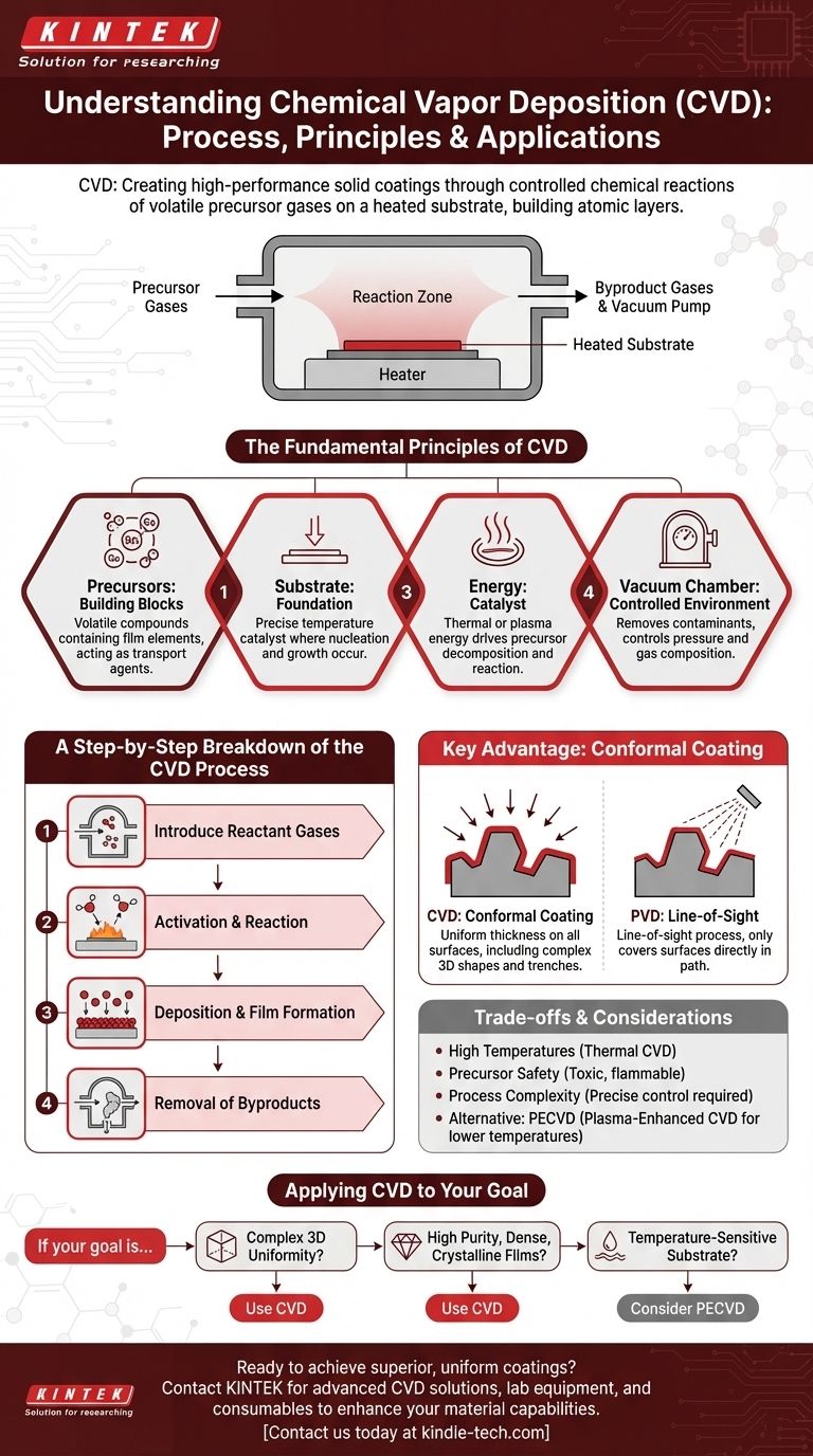
At its core, Chemical Vapor Deposition (CVD) is a process for creating a high-performance solid coating on a material's surface. This is achieved by introducing volatile precursor gases into a reaction chamber, which are then heated. The heat causes these gases to undergo a chemical reaction or decompose, forming a solid material that deposits and bonds onto the target surface, building a new layer atom by atom.
The true power of CVD is not merely coating a surface, but fundamentally transforming it by growing a new, highly-engineered solid material directly from a chemical vapor. Its key advantage is the ability to create an exceptionally uniform, or "conformal," coating that covers every exposed feature of a complex part.
The Fundamental Principles of CVD
To truly understand CVD, you must think of it as controlled chemical manufacturing on a microscopic scale. The process hinges on several key components working in a highly controlled environment.
The Role of Precursors: The Building Blocks
Precursors are the starting ingredients. They are volatile chemical compounds, often organometallics or halides, that are in a gaseous state at the process temperature.
These gases are carefully selected to contain the specific elements required for the final film. They are the transport mechanism, carrying the atomic building blocks into the reaction chamber.
The Substrate: The Foundation for Growth
The substrate is simply the part or material you intend to coat. During the CVD process, it is heated to a precise temperature.
This heated surface acts as the catalyst and foundation for the chemical reaction. The reaction occurs directly on or very near the substrate, which is where the new solid material nucleates and grows.
Energy as the Catalyst for Transformation
Energy, most often in the form of heat, is what drives the entire process. It provides the activation energy needed for the precursor gases to break their chemical bonds and react.
By precisely controlling the temperature, you can control the rate and type of chemical reaction, which in turn determines the properties of the final deposited film.
The Vacuum Chamber: A Controlled Environment
The entire process takes place within a reaction chamber, which is typically held under vacuum.
Creating a vacuum is critical for two reasons: it removes any air, moisture, or contaminants that could interfere with the reaction, and it allows for precise control over the pressure and composition of the precursor gas atmosphere.
A Step-by-Step Breakdown of the CVD Process
While the specific parameters vary widely, the core sequence of events in a thermal CVD process is consistent and logical.
Step 1: Introduction of Reactant Gases
The process begins by feeding a precisely controlled flow of one or more volatile precursor gases into the evacuated reaction chamber containing the substrate.
Step 2: Activation and Reaction
The substrate is heated to the target reaction temperature. As the precursor gases come into contact with the hot surface, they gain enough thermal energy to react with each other or to decompose into their constituent elements.
Step 3: Deposition and Film Formation
The product of this chemical reaction is a new, nonvolatile solid material. This solid deposits onto the hot substrate, forming a stable nucleus.
Over time, this process continues, and the solid material builds up layer by layer, forming a thin, dense, and uniform film across the entire surface.
Step 4: Removal of Byproducts
The chemical reactions often create other gaseous byproducts that are not part of the desired film. These waste gases are continuously removed from the chamber by the vacuum system.
Understanding the Key Advantage: Conformal Coating
The most significant distinction of CVD is its ability to produce a conformal coating, a characteristic that sets it apart from many other deposition techniques.
What "Conformal" Means
A conformal coating is one that follows the exact topography of the substrate with a uniform thickness. It covers ledges, trenches, and complex 3D shapes evenly.
Think of it like a gentle snowfall that blankets an entire landscape perfectly, in contrast to a directional spray that only hits the surfaces it can see.
CVD vs. PVD: A Critical Distinction
This multidirectional deposition is a key differentiator from Physical Vapor Deposition (PVD). PVD is a "line-of-sight" process, where coating material travels in a straight line from the source to the substrate.
Because CVD relies on a gas that fills the entire chamber, the chemical reaction and deposition happen on all heated surfaces, regardless of their orientation to the gas inlet.
The Trade-offs and Considerations of CVD
While powerful, CVD is not a universal solution. Understanding its limitations is crucial for making an informed decision.
High Temperatures
Traditional thermal CVD often requires very high temperatures to activate the chemical reactions. These temperatures can exceed the tolerance of many substrate materials, such as plastics or certain metal alloys.
Precursor Chemistry and Safety
The precursor gases used in CVD can be highly toxic, flammable, or corrosive. This necessitates sophisticated safety protocols, handling equipment, and exhaust management systems.
Process Complexity
Achieving a specific film with desired properties (e.g., crystalline structure, purity, hardness) requires extremely precise control over numerous variables, including temperature, pressure, gas flow rates, and chamber chemistry.
An Alternative: Plasma-Enhanced CVD (PECVD)
To overcome the high-temperature limitation, variants like Plasma-Enhanced CVD (PECVD) were developed. PECVD uses an electric field to generate a plasma, an energized state of matter.
This plasma provides the energy to drive the chemical reaction, allowing deposition to occur at much lower temperatures than in thermal CVD.
Applying CVD to Your Goal
Your choice to use CVD should be directly tied to the technical requirements of your final product.
- If your primary focus is coating complex 3D shapes uniformly: CVD is an exceptional choice due to its non-line-of-sight, conformal deposition capability.
- If you need to deposit highly pure, dense, or crystalline films: The controlled chemical reaction of CVD allows for precise engineering of material properties that are often unachievable with other methods.
- If your substrate is temperature-sensitive: You must consider lower-temperature variants like Plasma-Enhanced CVD (PECVD) to avoid material damage.
Ultimately, mastering CVD is about controlling chemistry in the vapor phase to build superior materials from the atom up.
Summary Table:
| Key CVD Process Component | Function |
|---|---|
| Precursor Gases | Supply the chemical building blocks for the film in a gaseous state. |
| Heated Substrate | Acts as the catalyst and foundation for the chemical reaction and film growth. |
| Vacuum Chamber | Provides a controlled, contaminant-free environment for the reaction. |
| Thermal/Plasma Energy | Drives the chemical reaction, decomposing the precursors to form the solid film. |
Ready to achieve superior, uniform coatings on your most complex components?
At KINTEK, we specialize in advanced CVD solutions for laboratory and industrial applications. Our expertise in lab equipment and consumables ensures you get the precise, high-performance coatings your projects demand, from durable protective layers to specialized functional films.
Let our team help you select the right CVD system for your specific substrate and coating requirements. Contact us today to discuss your application and discover how KINTEK can enhance your material capabilities.
Visual Guide
Related Products
- Chemical Vapor Deposition CVD Equipment System Chamber Slide PECVD Tube Furnace with Liquid Gasifier PECVD Machine
- Microwave Plasma Chemical Vapor Deposition MPCVD Machine System Reactor for Lab and Diamond Growth
- 915MHz MPCVD Diamond Machine Microwave Plasma Chemical Vapor Deposition System Reactor
- Customer Made Versatile CVD Tube Furnace Chemical Vapor Deposition Chamber System Equipment
- HFCVD Machine System Equipment for Drawing Die Nano-Diamond Coating
People Also Ask
- What are the core advantages of PE-CVD in OLED encapsulation? Protect Sensitive Layers with Low-Temp Film Deposition
- Why is Chemical Vapor Deposition (CVD) equipment uniquely suited for constructing hierarchical superhydrophobic structures?
- How expensive is chemical vapor deposition? Understanding the True Cost of High-Performance Coating
- What are the advantages of chemical vapor deposition? Achieve Superior Thin Films for Your Lab
- What are the processes of vapor phase deposition? Understand CVD vs. PVD for Superior Thin Films


