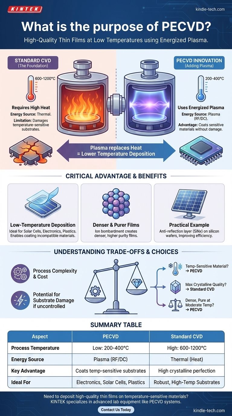
The primary purpose of Plasma-Enhanced Chemical Vapor Deposition (PECVD) is to deposit high-quality thin films onto a substrate at significantly lower temperatures than traditional methods. It achieves this by using an energized plasma to drive the chemical reactions needed to form the film, eliminating the need for the intense heat required by conventional Chemical Vapor Deposition (CVD). This makes it possible to coat materials that would otherwise be damaged or destroyed by high-temperature processing.
PECVD solves a critical manufacturing problem: how to create durable, pure thin films without damaging the underlying component with heat. By using plasma as an energy source instead of thermal energy, it enables the advanced fabrication of modern electronics, solar cells, and other temperature-sensitive devices.
Understanding the Foundation: Standard CVD
The Core Principle: Gaseous Reactions
Chemical Vapor Deposition (CVD) is a process used to create very thin, solid films on a surface, often called a substrate. It works by introducing one or more volatile precursor gases into a vacuum chamber.
The Key Requirement: High Heat
In standard CVD, the chamber is heated to a very high temperature. This heat provides the energy needed to break down the precursor gases, causing a chemical reaction that deposits the desired material onto the substrate, building a film layer by layer.
The Inherent Limitation
This reliance on high heat means standard CVD cannot be used on substrates that have low melting points or are otherwise sensitive to thermal damage, such as many plastics or complex electronic components.
The Innovation of PECVD: Adding Plasma to the Mix
How Plasma Changes the Equation
PECVD is an advanced form of CVD that adds a crucial element: plasma. A plasma is a state of matter created by applying energy (often radio frequency) to a gas, which ionizes it and creates a highly reactive environment.
This plasma provides the energy to break down the precursor gases, effectively replacing the need for extreme thermal energy. The chemical reactions can now occur at much lower temperatures.
The Critical Advantage: Low-Temperature Deposition
The ability to deposit films at low temperatures is the defining purpose of PECVD. This opens up the possibility of coating a vast range of materials that are incompatible with the harsh conditions of traditional CVD.
A Practical Example: Solar Cells
A common application is depositing a silicon nitride (SiNx) film onto a silicon wafer for solar panels. This film acts as an anti-reflection layer, reducing light reflection and improving the cell's energy conversion efficiency. PECVD is ideal because it creates the film without damaging the delicate silicon wafer with excessive heat.
Secondary Benefits: Purity and Density
The process also offers other advantages. The ion bombardment from the plasma onto the substrate during deposition can help create films that are denser and purer than those produced by other low-temperature methods.
Understanding the Trade-offs
Process Complexity
The main trade-off is increased complexity. PECVD systems require sophisticated equipment to generate and control the plasma, including RF or DC power sources, which can make the process more expensive and intricate to manage than standard thermal CVD.
Potential for Substrate Damage
While PECVD avoids thermal damage, the high-energy plasma itself can cause other types of damage to sensitive substrates if not carefully controlled. Fine-tuning the process parameters is critical to balance reaction efficiency with substrate integrity.
Film Characteristics
For certain applications requiring the highest possible crystalline perfection, high-temperature thermal CVD may still produce a superior film. The extreme heat of thermal CVD can promote better crystal growth for materials that can withstand the temperature.
Making the Right Choice for Your Goal
Choosing the correct deposition method depends entirely on the requirements of your substrate and the desired properties of the final film.
- If your primary focus is coating a temperature-sensitive material: PECVD is the definitive and often only choice.
- If your primary focus is achieving maximum crystalline quality on a robust substrate: Traditional high-temperature CVD may be the superior option.
- If your primary focus is creating dense, pure films at moderate temperatures: PECVD provides an excellent balance of film quality and process flexibility.
Ultimately, understanding the role of plasma as an energy substitute for heat is the key to selecting the right tool for your engineering challenge.
Summary Table:
| Aspect | PECVD | Standard CVD |
|---|---|---|
| Process Temperature | Low (e.g., 200-400°C) | High (e.g., 600-1200°C) |
| Energy Source | Plasma (RF/DC) | Thermal (heat) |
| Key Advantage | Coats temperature-sensitive substrates | High crystalline perfection |
| Ideal For | Electronics, solar cells, plastics | Robust, high-temperature substrates |
Need to deposit high-quality thin films on temperature-sensitive materials? KINTEK specializes in advanced lab equipment like PECVD systems, delivering precise, low-temperature deposition solutions for electronics, solar cells, and more. Let our experts help you enhance your fabrication process—contact us today to discuss your specific needs!
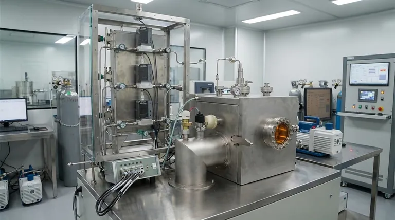
Visual Guide
Related Products
- Chemical Vapor Deposition CVD Equipment System Chamber Slide PECVD Tube Furnace with Liquid Gasifier PECVD Machine
- RF PECVD System Radio Frequency Plasma-Enhanced Chemical Vapor Deposition RF PECVD
- Inclined Rotary Plasma Enhanced Chemical Vapor Deposition PECVD Equipment Tube Furnace Machine
- Inclined Rotary Plasma Enhanced Chemical Vapor Deposition PECVD Equipment Tube Furnace Machine
- 915MHz MPCVD Diamond Machine Microwave Plasma Chemical Vapor Deposition System Reactor
People Also Ask
- How are carbon nanotubes grown? Master Scalable Production with Chemical Vapor Deposition
- How expensive is chemical vapor deposition? Understanding the True Cost of High-Performance Coating
- What types of substrates are used in CVD to facilitate graphene films? Optimize Graphene Growth with the Right Catalyst
- What is the chemical vapor deposition growth process? Build Superior Thin Films from the Atom Up
- What is plasma enhanced chemical vapor deposition PECVD equipment? A Guide to Low-Temperature Thin Film Deposition


