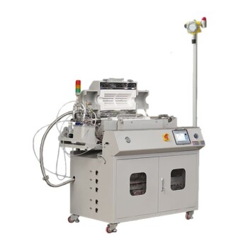
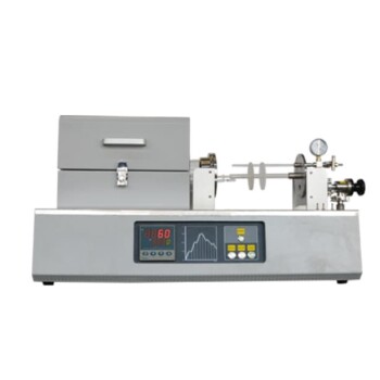
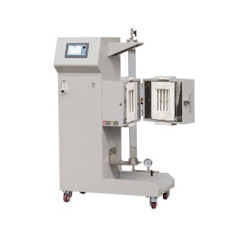
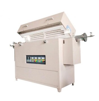
Nitrogen annealing is a critical post-deposition refinement process.
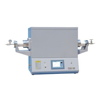
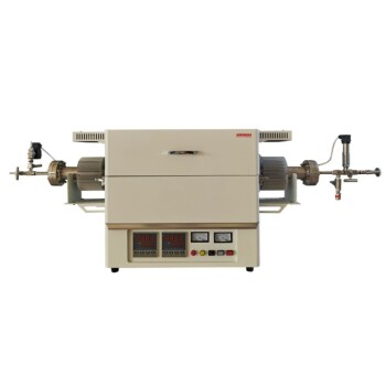
The primary purpose of performing nitrogen annealing on Cd-Ge-Se thin films is to eliminate residual stresses generated during rapid deposition and to stabilize the material's internal structure. By using a controlled tube furnace environment at temperatures between 473K and 573K, this treatment prevents thermal oxidation and ensures the stability of the film’s optical energy gap.
This thermal treatment serves as a dual-purpose stabilization step: it provides the energy required for structural relaxation while utilizing an inert nitrogen atmosphere to shield the chemically sensitive thin film from atmospheric degradation.
Structural Stabilization and Stress Relief
Eliminating Residual Internal Stresses
During the rapid deposition of thin films, atoms are often "frozen" into non-equilibrium positions, creating significant internal tension. Annealing provides the thermal energy necessary for these atoms to shift into more stable, lower-energy configurations.
This process of stress relief is vital for preventing future defects. Without it, internal stresses can lead to micro-cracks or film peeling, which compromises the mechanical integrity of the semiconductor layer.
Promoting Atomic Rearrangement
Thermal treatment encourages atomic rearrangement within the Cd-Ge-Se matrix. This often involves a transition from a metastable or amorphous state toward a more ordered polycrystalline structure.
Improved crystallinity typically leads to better electronic properties. By reducing structural disorders, the film can achieve higher carrier mobility and more predictable photovoltaic responses.
The Role of the Controlled Nitrogen Atmosphere
Preventing Thermal Oxidation
Cd-Ge-Se compounds are highly susceptible to reacting with oxygen when heated in an open environment. The tube furnace allows for the introduction of high-purity nitrogen, which flushes out oxygen and moisture.
Creating this inert shield prevents the formation of unwanted oxide layers on the film surface. Maintaining chemical purity is essential for ensuring that the resulting device behaves according to its intended stoichiometric design.
Ensuring Optical Energy Gap Stability
The optical energy gap is a fundamental property that dictates how the thin film interacts with light. Thermal oxidation or structural inconsistencies can cause this gap to shift unpredictably.
By annealing under nitrogen, the stability of the optical energy gap is preserved. This allows researchers to isolate experimental variables and ensure that the material's light-absorption characteristics remain consistent.
Understanding the Trade-offs and Pitfalls
Temperature Precision Requirements
The window for effective annealing is relatively narrow, typically between 473K and 573K. If the temperature is too low, the internal stresses will remain, leaving the film brittle and unstable.
Conversely, excessive heat can lead to the desorption of volatile elements like Selenium. This "over-annealing" can result in compositional non-uniformity, fundamentally changing the semiconductor's electrical behavior.
Atmosphere Purity Risks
The success of the process depends entirely on the purity of the nitrogen flow. Even trace amounts of oxygen or water vapor within the tube furnace can cause localized oxidation.
System leaks or impure gas sources can introduce "pinhole" defects. These defects act as recombination centers for charge carriers, significantly reducing the efficiency of the thin film in practical applications.
How to Optimize the Annealing Process
The ideal annealing strategy depends on the specific requirements of your semiconductor application and the deposition method used.
- If your primary focus is mechanical durability: Prioritize a longer dwell time at the lower end of the temperature range (473K) to allow for gradual stress relaxation without risking film peeling.
- If your primary focus is optical precision: Ensure a high-velocity nitrogen purge before heating begins to guarantee a completely oxygen-free environment, protecting the energy gap.
- If your primary focus is electrical conductivity: Target the higher end of the temperature range (573K) to maximize atomic rearrangement and crystallinity, provided the film's composition remains stable.
By carefully balancing thermal energy with atmosphere control, you can transform a raw deposited layer into a high-performance, stable semiconductor component.
Summary Table:
| Key Purpose | Detailed Benefit of Nitrogen Annealing |
|---|---|
| Stress Relief | Eliminates residual internal tension to prevent micro-cracks and film peeling. |
| Oxidation Prevention | High-purity nitrogen shield flushes out oxygen to maintain chemical purity. |
| Structural Relaxation | Encourages atomic rearrangement for improved crystallinity and carrier mobility. |
| Energy Gap Stability | Preserves the optical energy gap for consistent light-absorption characteristics. |
| Thermal Precision | Controlled heating (473K-573K) ensures stability without element desorption. |
Optimize Your Semiconductor Research with KINTEK Thermal Solutions
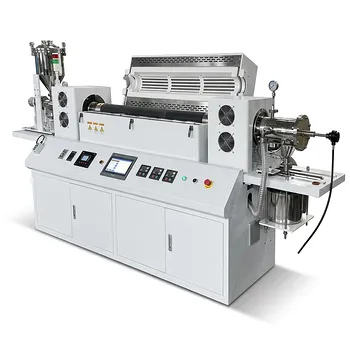
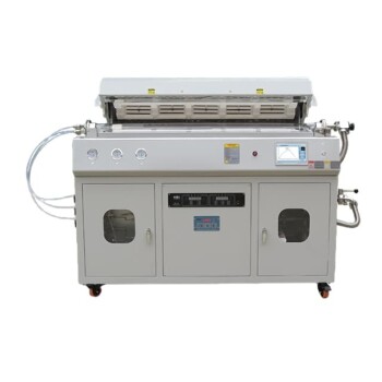
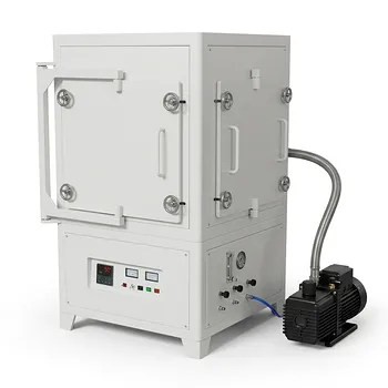
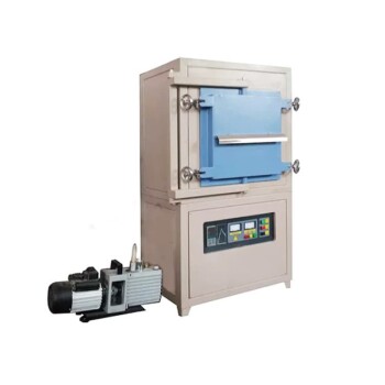
Achieving the perfect annealing environment for Cd-Ge-Se thin films requires uncompromising temperature precision and atmosphere purity. KINTEK specializes in advanced laboratory equipment, offering high-performance tube furnaces, vacuum furnaces, and CVD systems designed for the most sensitive material refinement processes.
Our extensive portfolio supports every stage of your workflow:
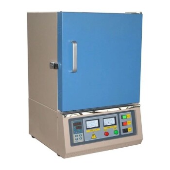
- Thermal Processing: Muffle, tube, and atmosphere furnaces for precise heat treatments.
- Material Preparation: Crushing, milling systems, and hydraulic pellet presses.
- Specialized Reactors: High-temperature high-pressure reactors and autoclaves.
- Lab Essentials: Cooling solutions (ULT freezers), electrolytic cells, and high-quality consumables like PTFE and ceramics.
Ready to enhance your material stability and lab efficiency? Contact KINTEK today to discover how our tailored equipment solutions can drive your next breakthrough!
References
- Abdel-naser A. Alfaqeer, M. A. Dabban. Implications of Changing the Cd-Ge-Se Thin Film Thickness Deposited by Thermal Evaporation Technique on Structural and Optical Properties for Optoelectronic Applications. DOI: 10.5281/zenodo.7765619
This article is also based on technical information from Kintek Solution Knowledge Base .
Related Products
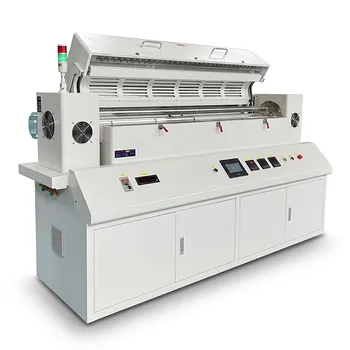
- Rotary Tube Furnace Split Multi Heating Zone Rotating Tube Furnace
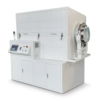
- Laboratory Vacuum Tilt Rotary Tube Furnace Rotating Tube Furnace
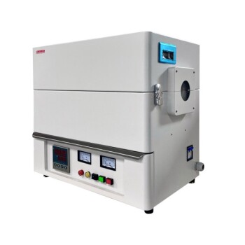
- 1200℃ Split Tube Furnace with Quartz Tube Laboratory Tubular Furnace
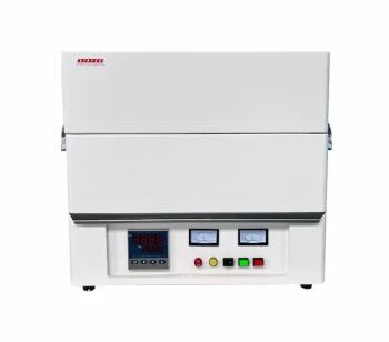
- 1400℃ Laboratory High Temperature Tube Furnace with Alumina Tube
- 1700℃ Laboratory High Temperature Tube Furnace with Alumina Tube
People Also Ask
- What are the process advantages of using a rotary tube furnace for WS2 powder? Achieve Superior Material Crystallinity
- What are the advantages of using a rotary tube furnace for MoVOx catalysts? Elevate Uniformity and Crystallinity
- Why is a rotary tube furnace preferred over a fixed tube furnace for the carbonization of asphaltenes? Superior Quality
- What is a rotary tube furnace? Achieve Superior Uniformity for Powders and Granules
- Why is a rotary tube furnace recommended for the calcination stage of potassium vanadium oxide catalysts? Optimize Purity