The significance of good conformal step coverage lies in its ability to maintain consistent film thickness across complex, uneven geometries. Unlike basic line-of-sight deposition, Plasma Enhanced Chemical Vapor Deposition (PECVD) ensures that material builds up uniformly on both flat surfaces and vertical step edges.
In microfabrication, reliable step coverage is the difference between a functional device and a failed one. It ensures that protective or conductive layers remain continuous over "steps" and distinct features, preventing electrical shorts and mechanical cracking.
Ensuring Structural Integrity
Uniformity Over Edges
The primary function of conformal step coverage is geometric consistency. In many deposition processes, films tend to thin out at sharp corners or build up excessively on top surfaces while neglecting sidewalls.
PECVD mitigates this by utilizing plasma to drive chemical reactions. This results in a film that wraps around step edges with nearly the same thickness as it has on flat areas.
Handling Substrate Topography
Modern device fabrication rarely involves perfectly flat surfaces. Substrates often feature "steps," trenches, or patterned relief structures.
Good step coverage allows you to deposit films onto these uneven surfaces without leaving gaps or keyholes. This is critical for multilayer devices where subsequent layers depend on the smoothness and continuity of the layers beneath them.
Enhancing Film Quality and Reliability
Preventing Mechanical Failure
Films that lack conformal coverage are prone to structural weaknesses. If a coating is too thin at a step edge, it creates a stress concentration point.
Because PECVD layers provide superior consistency, they are significantly less likely to crack. This mechanical robustness is essential for the long-term durability of the component.
Superiority Over Conventional CVD
Standard Chemical Vapor Deposition (CVD) often struggles with consistency on irregular shapes. PECVD offers superior consistency and coverage on these difficult topologies.
This advantage enables the creation of high-quality films that maintain their integrity even when deposited over substantial topographic variations.
Understanding the Trade-offs
Application Suitability
While PECVD offers excellent coverage, it is important to match the method to the specific geometry.
For extremely high-aspect-ratio trenches (deep and narrow holes), even PECVD has limits compared to slower methods like Atomic Layer Deposition (ALD). However, for general "stepped" features, PECVD provides the optimal balance of speed and coverage.
Process Control
Achieving perfect conformality requires precise control over the thin film process.
While PECVD allows for this control, aggressive deposition rates to achieve thick coatings (greater than 10 μm) must be balanced against the need for perfect step coverage to ensure the film does not close off at the top before filling the bottom of a step.
Making the Right Choice for Your Goal
To maximize the benefits of PECVD in your fabrication process, consider your specific constraints:
- If your primary focus is complex topography: Prioritize PECVD for its ability to maintain uniform thickness over step edges and uneven surfaces where standard CVD might fail.
- If your primary focus is film durability: Rely on the conformal nature of PECVD to produce low-stress layers that are resistant to cracking at corner interfaces.
- If your primary focus is heat-sensitive substrates: Leverage PECVD's ability to achieve this high-quality coverage at lower temperatures (room temperature to 350°C).
Good step coverage is not just about aesthetics; it is the fundamental requirement for electrical continuity and mechanical survival in structured devices.
Summary Table:
| Feature | PECVD Conformal Coverage Benefit |
|---|---|
| Geometric Consistency | Maintains uniform film thickness across flat surfaces and vertical sidewalls. |
| Structural Integrity | Prevents thinning at sharp corners, reducing stress concentration and cracking. |
| Topography Handling | Effectively fills trenches and patterned relief without gaps or 'keyholes'. |
| Process Versatility | Enables high-quality deposition on heat-sensitive substrates at lower temperatures. |
| Device Reliability | Ensures electrical continuity and mechanical durability in multi-layer structures. |
Elevate Your Microfabrication Precision with KINTEK
Don't let poor step coverage compromise your device performance. KINTEK specializes in advanced laboratory solutions, offering state-of-the-art PECVD, CVD, and MPCVD systems designed to achieve superior film uniformity and structural integrity on even the most complex substrates.
Whether you are working on battery research, semiconductor development, or high-temperature material science, our comprehensive portfolio—including high-temperature furnaces, hydraulic presses, and specialized electrolytic cells—provides the reliability your research demands.
Ready to optimize your deposition process? Contact our technical experts today to discover how KINTEK can enhance your lab's efficiency and film quality.
Related Products
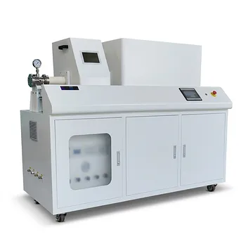
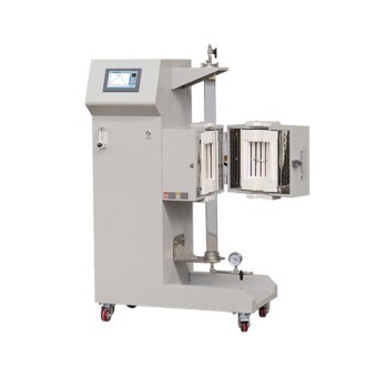
- Inclined Rotary Plasma Enhanced Chemical Vapor Deposition PECVD Equipment Tube Furnace Machine
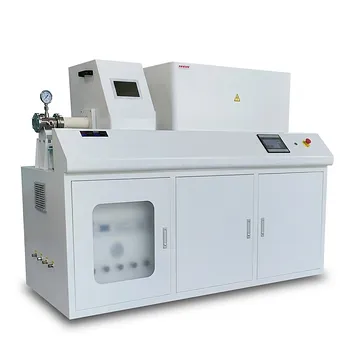
- Chemical Vapor Deposition CVD Equipment System Chamber Slide PECVD Tube Furnace with Liquid Gasifier PECVD Machine
- Inclined Rotary Plasma Enhanced Chemical Vapor Deposition PECVD Equipment Tube Furnace Machine
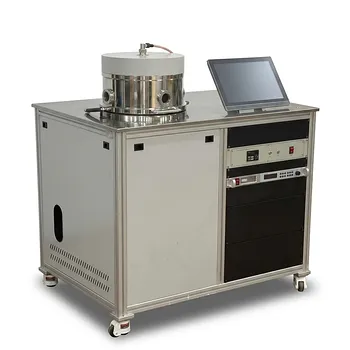
- RF PECVD System Radio Frequency Plasma-Enhanced Chemical Vapor Deposition RF PECVD
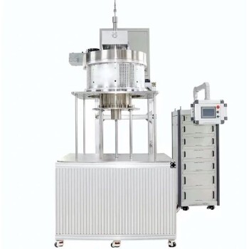
- Multi Heating Zones CVD Tube Furnace Machine Chemical Vapor Deposition Chamber System Equipment
People Also Ask
- What are the advantages of plasma enhanced chemical vapor deposition? Enable Low-Temperature, High-Quality Film Deposition
- How does PECVD equipment facilitate the directional growth of carbon nanotubes? Achieve Precision Vertical Alignment
- What is plasma enhanced chemical vapour deposition PECVD used for? Enable Low-Temp Thin Films for Electronics & Solar
- How does PECVD process work? Achieve Low-Temperature, High-Quality Thin Films
- What is plasma enhanced chemical vapor deposition PECVD equipment? A Guide to Low-Temperature Thin Film Deposition
