Knowledge What is the thickness of a metal layer? It Depends on Your Application, from Nanometers to Meters
Author avatar

Tech Team · Kintek Solution

Updated 6 days ago

What is the thickness of a metal layer? It Depends on Your Application, from Nanometers to Meters

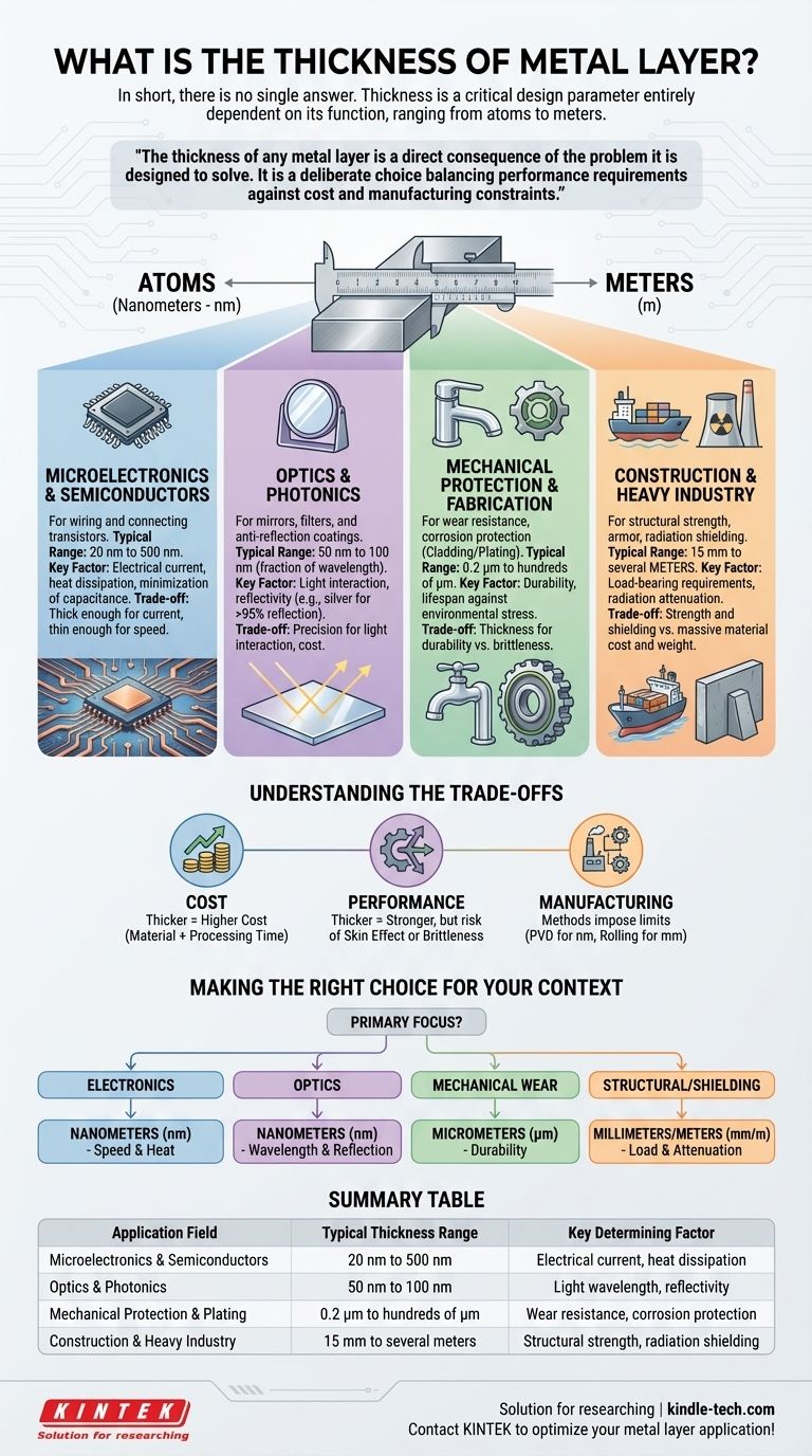
In short, there is no single answer. The thickness of a metal layer is not a fixed value but a critical design parameter that is entirely dependent on its intended function. This value can range from a few atoms thick in a semiconductor chip to several meters thick for radiation shielding in a nuclear facility.

The thickness of any metal layer is a direct consequence of the problem it is designed to solve. It is a deliberate choice balancing performance requirements—such as electrical conductivity, mechanical strength, or optical behavior—against the constraints of cost and manufacturing feasibility.

Why Application Determines Thickness

The term "metal layer" is used across dozens of industries, from microelectronics to heavy construction. The required thickness is dictated by the physical properties needed for the layer to perform its job successfully. A layer designed for electrical purposes has vastly different requirements than one designed for structural integrity.

For Microelectronics and Semiconductors

In integrated circuits, metal layers (like copper or aluminum) form the wiring that connects billions of transistors. Here, thickness is measured in nanometers (nm).

A typical range might be 20 nm to 500 nm. The thickness is a careful trade-off. It must be thick enough to carry the required electrical current without overheating (electromigration) but thin enough to minimize capacitance between layers, which would slow the chip down.

For Optics and Photonics

Metal layers are used to create mirrors or specialized filters. The thickness is chosen based on its interaction with light and is often a fraction of a specific wavelength.

For a highly reflective mirror, a silver or aluminum layer might be 50 nm to 100 nm thick. This is sufficient to be opaque and reflect over 95% of visible light. For anti-reflection coatings, much thinner, multi-layered films are used to create destructive interference.

For Mechanical Protection and Fabrication

In manufacturing, metal layers provide wear resistance, corrosion protection, or a base for further processing. This is often called cladding or plating.

Thickness here is measured in micrometers (µm), also known as microns. A chrome plating on a faucet for corrosion resistance might be 0.2 µm to 0.5 µm, while a hard-facing layer on an industrial tool could be hundreds of micrometers thick.

For Construction and Heavy Industry

In large-scale applications, metal layers provide structural strength, armor, or containment. Thickness is measured in millimeters (mm) or centimeters (cm).

The steel plate hull of a cargo ship can be 15 mm to 25 mm thick. The steel and lead layers in a nuclear reactor's containment vessel can be several meters thick to provide radiation shielding.

Understanding the Trade-offs: Cost, Performance, and Process

Choosing a layer's thickness is never done in a vacuum. It involves a critical balance of competing factors that every engineer must consider.

Cost vs. Thickness

Thicker layers almost always mean higher costs. This is due not only to the increased amount of raw material (like gold or platinum) but also to the longer processing time required for deposition, plating, or rolling.

Performance Degradation

While thicker can mean stronger, it can also harm performance. In high-frequency electronics, a phenomenon called the "skin effect" causes current to flow only on the outer surface of a conductor, making a thick wire act like a thin one and wasting material. An overly thick coating can also be brittle and prone to cracking.

Manufacturing Limitations

The method used to create the layer imposes its own limits. Physical Vapor Deposition (PVD) is excellent for creating uniform, nanometer-scale films but is too slow and expensive for millimeter-thick layers. Rolling and welding are efficient for thick plates but lack the precision for optical coatings.

Making the Right Choice for Your Context

To determine the relevant thickness, you must first identify the primary function of the layer within your specific field.

  • If your primary focus is electronics or semiconductors: Thickness will be in nanometers, dictated by signal speed, current density, and heat dissipation.
  • If your primary focus is optics: Thickness will be in nanometers, determined by the target wavelength of light for reflection, absorption, or interference.
  • If your primary focus is mechanical wear or corrosion: Thickness will be in micrometers, chosen for durability and lifespan against a specific environmental stress.
  • If your primary focus is structural integrity or shielding: Thickness will be in millimeters or centimeters, calculated based on load-bearing requirements or radiation attenuation properties.

Ultimately, the thickness of a metal layer is a precise answer to a specific engineering question.

Summary Table:

Application Field Typical Thickness Range Key Determining Factor
Microelectronics & Semiconductors 20 nm to 500 nm Electrical current, heat dissipation
Optics & Photonics 50 nm to 100 nm Light wavelength, reflectivity
Mechanical Protection & Plating 0.2 µm to hundreds of µm Wear resistance, corrosion protection
Construction & Heavy Industry 15 mm to several meters Structural strength, radiation shielding

Struggling to determine the optimal metal layer thickness for your specific application? The right thickness is critical for performance, cost, and manufacturability. KINTEK specializes in lab equipment and consumables for precise material deposition and analysis, serving industries from microelectronics to heavy manufacturing. Our experts can help you select the right equipment and processes to achieve your desired layer properties. Contact our team today to discuss your project requirements and optimize your metal layer application!

Related Products

People Also Ask

Related Products

RF PECVD System Radio Frequency Plasma-Enhanced Chemical Vapor Deposition RF PECVD

RF PECVD System Radio Frequency Plasma-Enhanced Chemical Vapor Deposition RF PECVD

RF-PECVD is an acronym for "Radio Frequency Plasma-Enhanced Chemical Vapor Deposition." It deposits DLC (Diamond-like carbon film) on germanium and silicon substrates. It is utilized in the 3-12um infrared wavelength range.

Inclined Rotary Plasma Enhanced Chemical Vapor Deposition PECVD Equipment Tube Furnace Machine

Inclined Rotary Plasma Enhanced Chemical Vapor Deposition PECVD Equipment Tube Furnace Machine

Upgrade your coating process with PECVD coating equipment. Ideal for LED, power semiconductors, MEMS and more. Deposits high-quality solid films at low temps.

Electron Beam Evaporation Coating Oxygen-Free Copper Crucible and Evaporation Boat

Electron Beam Evaporation Coating Oxygen-Free Copper Crucible and Evaporation Boat

Electron Beam Evaporation Coating Oxygen-Free Copper Crucible enables precise co-deposition of various materials. Its controlled temperature and water-cooled design ensure pure and efficient thin film deposition.

Chemical Vapor Deposition CVD Equipment System Chamber Slide PECVD Tube Furnace with Liquid Gasifier PECVD Machine

Chemical Vapor Deposition CVD Equipment System Chamber Slide PECVD Tube Furnace with Liquid Gasifier PECVD Machine

KT-PE12 Slide PECVD System: Wide power range, programmable temp control, fast heating/cooling with sliding system, MFC mass flow control & vacuum pump.

Microwave Plasma Chemical Vapor Deposition MPCVD Machine System Reactor for Lab and Diamond Growth

Microwave Plasma Chemical Vapor Deposition MPCVD Machine System Reactor for Lab and Diamond Growth

Get high-quality diamond films with our Bell-jar Resonator MPCVD machine designed for lab and diamond growth. Discover how Microwave Plasma Chemical Vapor Deposition works for growing diamonds using carbon gas and plasma.

CVD Diamond for Thermal Management Applications

CVD Diamond for Thermal Management Applications

CVD diamond for thermal management: High-quality diamond with thermal conductivity up to 2000 W/mK, ideal for heat spreaders, laser diodes, and GaN on Diamond (GOD) applications.

Customer Made Versatile CVD Tube Furnace Chemical Vapor Deposition Chamber System Equipment

Customer Made Versatile CVD Tube Furnace Chemical Vapor Deposition Chamber System Equipment

Get your exclusive CVD furnace with KT-CTF16 Customer Made Versatile Furnace. Customizable sliding, rotating, and tilting functions for precise reactions. Order now!

CVD Diamond Domes for Industrial and Scientific Applications

CVD Diamond Domes for Industrial and Scientific Applications

Discover CVD diamond domes, the ultimate solution for high-performance loudspeakers. Made with DC Arc Plasma Jet technology, these domes deliver exceptional sound quality, durability, and power handling.

VHP Sterilization Equipment Hydrogen Peroxide H2O2 Space Sterilizer

VHP Sterilization Equipment Hydrogen Peroxide H2O2 Space Sterilizer

A hydrogen peroxide space sterilizer is a device that uses vaporized hydrogen peroxide to decontaminate enclosed spaces. It kills microorganisms by damaging their cellular components and genetic material.

Cylindrical Resonator MPCVD Machine System Reactor for Microwave Plasma Chemical Vapor Deposition and Lab Diamond Growth

Cylindrical Resonator MPCVD Machine System Reactor for Microwave Plasma Chemical Vapor Deposition and Lab Diamond Growth

Learn about Cylindrical Resonator MPCVD Machine, the microwave plasma chemical vapor deposition method used for growing diamond gemstones and films in the jewelry and semi-conductor industries. Discover its cost-effective advantages over traditional HPHT methods.

Single Punch Electric Tablet Press Machine Laboratory Powder Tablet Punching TDP Tablet Press

Single Punch Electric Tablet Press Machine Laboratory Powder Tablet Punching TDP Tablet Press

The single-punch electric tablet press is a laboratory-scale tablet press suitable for corporate laboratories in pharmaceutical, chemical, food, metallurgical and other industries.

Non Consumable Vacuum Arc Induction Melting Furnace

Non Consumable Vacuum Arc Induction Melting Furnace

Explore the benefits of Non-Consumable Vacuum Arc Furnace with high melting point electrodes. Small, easy to operate & eco-friendly. Ideal for laboratory research on refractory metals & carbides.

High Performance Laboratory Freeze Dryer

High Performance Laboratory Freeze Dryer

Advanced lab freeze dryer for lyophilization, preserving biological & chemical samples efficiently. Ideal for biopharma, food, and research.

High Performance Laboratory Freeze Dryer for Research and Development

High Performance Laboratory Freeze Dryer for Research and Development

Advanced laboratory freeze dryer for lyophilization, preserving sensitive samples with precision. Ideal for biopharmaceuticals, research & food industries.

Platinum Sheet Electrode for Laboratory and Industrial Applications

Platinum Sheet Electrode for Laboratory and Industrial Applications

Elevate your experiments with our Platinum Sheet Electrode. Crafted with quality materials, our safe and durable models can be tailored to fit your needs.

Laboratory Vibratory Sieve Shaker Machine Slap Vibrating Sieve

Laboratory Vibratory Sieve Shaker Machine Slap Vibrating Sieve

KT-T200TAP is a slapping and oscillating sieving instrument for laboratory desktop use, with 300 rpm horizontal circular motion and 300 vertical slapping motions to simulate manual sieving to help sample particles pass through better.

Rotating Platinum Disk Electrode for Electrochemical Applications

Rotating Platinum Disk Electrode for Electrochemical Applications

Upgrade your electrochemical experiments with our Platinum Disc Electrode. High-quality and reliable for accurate results.

Assemble Square Lab Press Mold for Laboratory Applications

Assemble Square Lab Press Mold for Laboratory Applications

Achieve perfect sample preparation with Assemble Square Lab Press Mold. Quick disassembly eliminates sample deformation. Perfect for battery, cement, ceramics, and more. Customizable sizes available.

Evaporation Crucible for Organic Matter

Evaporation Crucible for Organic Matter

An evaporation crucible for organic matter, referred to as an evaporation crucible, is a container for evaporating organic solvents in a laboratory environment.

Assemble Lab Cylindrical Press Mold

Assemble Lab Cylindrical Press Mold

Get reliable and precise molding with Assemble Lab Cylindrical Press Mold. Perfect for ultra-fine powder or delicate samples, widely used in material research and development.


Leave Your Message