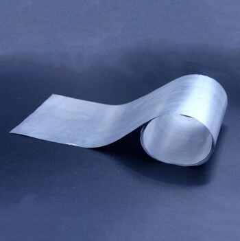
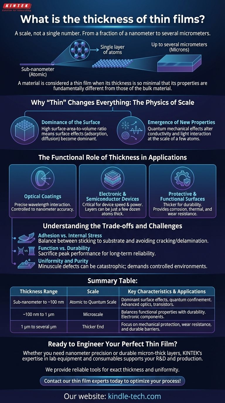
At its core, a thin film's thickness is defined by a scale, not a single number. This range spans from a fraction of a nanometer—equivalent to a single layer of atoms—up to several micrometers (microns). A material is considered a thin film when its thickness is so minimal that its properties are fundamentally different from those of the bulk material.
The critical takeaway is that "thin film" describes a physical state where the material's behavior is governed by surface-level physics and quantum effects, not its bulk properties. The precise thickness is engineered to unlock specific optical, electrical, or mechanical functions that would otherwise be impossible.
Why "Thin" Changes Everything: The Physics of Scale
The unique properties of thin films arise because, at this scale, the normal rules of a material don't apply. Two key factors come into play.
The Dominance of the Surface
In any bulk material, the vast majority of atoms are surrounded by other atoms. In a thin film, a significant percentage of atoms are on a surface or at an interface with another material.
This dramatically high surface-area-to-volume ratio means that surface effects, such as adsorption and diffusion, which are negligible in bulk materials, become dominant forces that define the film's characteristics.
The Emergence of New Properties
When a film's thickness approaches the scale of a few atoms, its physical properties can change entirely.
The behavior of electrons is no longer averaged over a large volume but is confined to a tiny space. This can lead to quantum mechanical effects that alter a material's conductivity or its interaction with light, creating opportunities for new technologies.
The Functional Role of Thickness in Applications
The required thickness of a film is dictated entirely by its intended function. A film designed for wear resistance will have a very different thickness than one designed for an anti-reflection coating.
Optical Coatings
For applications like anti-reflective coatings on lenses or reflective layers on mirrors, the thickness must be controlled with extreme precision.
The film's thickness is engineered to be a specific fraction of the wavelength of light it is meant to interact with, often requiring accuracy down to the nanometer.
Electronic and Semiconductor Devices
In integrated circuits, the thickness of insulating, conducting, and semiconducting layers is a critical design parameter.
The thickness of a silicon dioxide gate insulator in a transistor, for example, directly controls the device's switching speed and power consumption. These layers can be just a few dozen atoms thick.
Protective and Functional Surfaces
When used for protective purposes—such as providing corrosion resistance on metal parts, thermal barriers on turbine blades, or wear resistance on cutting tools—films are typically thicker.
These films often fall into the higher end of the range, from several hundred nanometers up to a few micrometers, to provide a durable and effective barrier.
Understanding the Trade-offs and Challenges
While thin films enable incredible technologies, their nature presents significant engineering challenges. The choice of thickness is always a balance of competing factors.
Adhesion vs. Internal Stress
A film is only useful if it sticks to the substrate. However, the process of depositing a film can build up internal stress, especially in thicker films. This stress can cause the film to crack, delaminate, or peel away, rendering it useless.
Function vs. Durability
An extremely thin film might possess ideal optical or electrical properties but be too fragile to survive its operating environment. Engineers must often sacrifice some peak performance for a slightly thicker, more robust film that guarantees long-term reliability.
Uniformity and Purity
Because the film is so thin, even a minuscule defect or impurity can be catastrophic. A single stray dust particle or a slight variation in thickness across a surface can ruin a semiconductor wafer or create a flaw in an optical lens. This demands highly controlled, clean manufacturing environments.
Making the Right Choice for Your Goal
The "correct" thickness is the one that achieves your specific technical goal while remaining manufacturable and reliable.
- If your primary focus is advanced optics: Thickness must be controlled with sub-nanometer precision to manipulate specific wavelengths of light.
- If your primary focus is semiconductor fabrication: Thickness directly controls the electronic properties of gates and conductive layers, defining device performance.
- If your primary focus is mechanical protection or durability: A thicker film (often in the micron range) is generally required for wear resistance, but you must balance this against internal stress and adhesion.
- If your primary focus is decorative coating: Thickness is chosen to achieve a desired color and appearance while ensuring it can withstand expected wear and tear.
Ultimately, a thin film's thickness is not just a dimension, but the fundamental parameter that defines its function and unlocks its potential.
Summary Table:
| Thickness Range | Scale | Key Characteristics & Applications |
|---|---|---|
| Sub-nanometer to ~100 nm | Atomic to Quantum Scale | Dominant surface effects, quantum confinement. Ideal for advanced optics (anti-reflective coatings) and semiconductor devices (transistor gates). |
| ~100 nm to 1 μm | Microscale | Balances functional properties with durability. Common for many electronic components and functional surfaces. |
| 1 μm to several μm | Thicker End | Focus on mechanical protection, wear resistance, and durable barriers (e.g., thermal barriers, corrosion protection). |
Ready to Engineer Your Perfect Thin Film?
The precise thickness of your thin film is the key to its performance. Whether you need nanometer precision for optical coatings or durable micron-thick layers for protection, KINTEK's expertise in lab equipment and consumables is here to support your R&D and production.
We provide the reliable tools and materials necessary to achieve the exact thickness and uniformity your application demands. Let's discuss your specific requirements and how we can help you succeed.
Contact our thin film experts today to optimize your process!
Visual Guide
Related Products
- RF PECVD System Radio Frequency Plasma-Enhanced Chemical Vapor Deposition RF PECVD
- Evaporation Boat for Organic Matter
- Vacuum Hot Press Furnace Machine for Lamination and Heating
- Custom PTFE Teflon Parts Manufacturer for Centrifuge Tube Racks
- Custom PTFE Teflon Parts Manufacturer for PTFE Mesh F4 Sieve
People Also Ask
- Why does PECVD commonly use RF power input? For Precise Low-Temperature Thin Film Deposition
- What are the advantages of PECVD? Enable Low-Temperature, High-Quality Thin-Film Deposition
- What is an example of PECVD? RF-PECVD for High-Quality Thin Film Deposition
- What are the benefits of PECVD? Achieve Superior Low-Temperature Thin Film Deposition
- Why is PECVD environment friendly? Understanding the Eco-Friendly Benefits of Plasma-Enhanced Coating