In semiconductor manufacturing, the thin film process is a foundational technique for building integrated circuits from the ground up. It is the highly controlled method of depositing an extremely thin, uniform layer of material—often just a few atoms thick—onto a substrate, typically a silicon wafer. This process is repeated dozens of times with different materials to construct the intricate, multi-layered structures that form transistors, wires, and other components of a microchip.
At its core, the thin film process isn't just about adding a layer; it's about precisely engineering the electrical properties of a microchip at the atomic scale. Mastering this is the difference between a simple piece of silicon and a powerful central processing unit.
Why Thin Films are the Bedrock of Modern Electronics
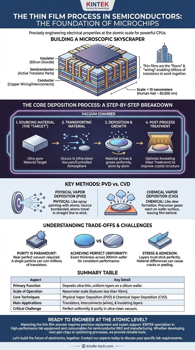
Building a Microscopic Skyscraper
An integrated circuit is not a flat, two-dimensional object. It is a dense, three-dimensional structure, like a microscopic skyscraper, with tens or even hundreds of layers.
Thin film deposition is the construction method used to build each "floor" and the "wiring" (interconnects) between them, allowing billions of transistors to work together.
Engineering Electrical Properties
The function of each layer is determined by the material deposited. Thin films of conductive materials like copper create wires, while insulating materials like silicon dioxide prevent electrical shorts.
Layers of specific semiconductor materials are deposited to create the active parts of transistors, which act as the chip's on/off switches.
The Scale of Unbelievable Precision
This process operates on a nanometer scale, which is difficult to comprehend. A single human hair is about 80,000 nanometers wide. Modern chip features built with thin films can be less than 10 nanometers.
Achieving this level of precision has taken over 60 years of cumulative scientific progress, requiring advances in physics, chemistry, and materials science.
The Core Deposition Process: A Step-by-Step Breakdown
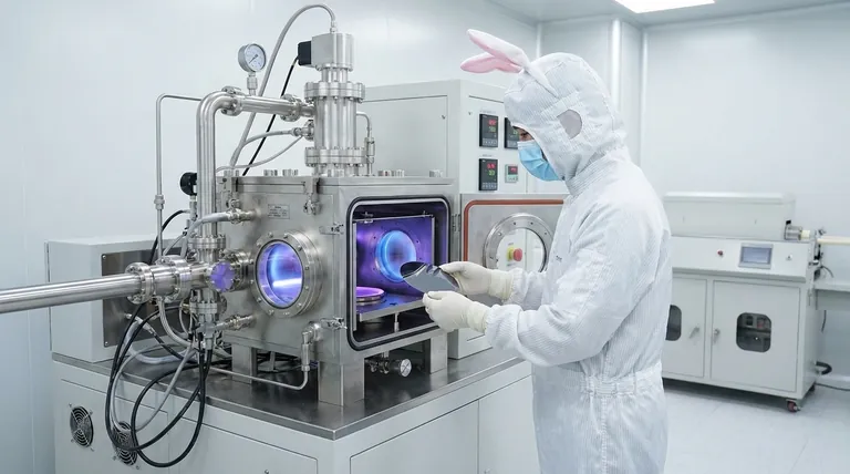
Nearly all thin film deposition techniques follow the same fundamental sequence, which takes place inside an ultra-clean vacuum chamber to prevent any contamination.
Step 1: Sourcing the Material (The "Target")
The process begins with a source of ultra-pure material that will form the new layer. This source is often called a target.
Step 2: Transporting Material to the Substrate
The atoms or molecules from the target material must be transported to the substrate (the silicon wafer).
This is the key step where different techniques vary, but it always occurs in a vacuum or a highly controlled atmosphere to ensure purity.
Step 3: Deposition and Growth
The transported material arrives at the wafer surface and begins to form a new, solid layer. This film grows uniformly, atom by atom, across the entire surface.
Step 4: Post-Process Treatment
In some cases, the wafer is subjected to a final treatment after deposition, such as annealing (a high-temperature heat treatment). This can improve the film's crystal structure and electrical characteristics.
Key Deposition Methods: PVD vs. CVD
While there are many specific techniques, they generally fall into two major families: Physical Vapor Deposition (PVD) and Chemical Vapor Deposition (CVD).
Physical Vapor Deposition (PVD)
PVD is a physical process. Think of it like spray painting, but with individual atoms. The source material is physically bombarded with energy (like an ion beam) to knock atoms loose.
These atoms then travel in a straight line through the vacuum chamber and stick to the wafer, forming the thin film.
Chemical Vapor Deposition (CVD)
CVD is a chemical process. An analogy is dew forming on a cold surface. Special precursor gases containing the desired atoms are introduced into the chamber.
These gases react on the hot surface of the wafer, and as a byproduct of that chemical reaction, a solid thin film is "left behind" on the surface.
Understanding the Trade-offs and Challenges
The theoretical process is simple, but practical implementation is incredibly difficult and defines the cutting edge of manufacturing technology.
Purity is Paramount
The entire process must occur in a near-perfect vacuum inside a sealed chamber. A single microscopic dust particle can land on the wafer and cause a defect that ruins thousands or millions of transistors.
Achieving Perfect Uniformity
The deposited film must have the exact same thickness across the entire 300mm wafer. Even a slight variation can cause different parts of the chip to perform differently, leading to failure.
Stress and Adhesion
Each new layer must stick perfectly to the one below it. Differences in material properties can create physical stress, leading to cracks or peeling that destroy the device. The choice of deposition method heavily influences these properties.
Making the Right Choice for Your Goal
The method chosen depends entirely on the material being deposited and its purpose within the final microchip.
- If your primary focus is on metallization (chip wiring): PVD is often the most direct and effective method for depositing pure metals like copper, aluminum, or titanium.
- If your primary focus is on high-quality dielectrics or semiconducting layers: CVD provides superior film quality, purity, and the ability to evenly coat complex 3D structures, making it essential for building transistor gates and insulating layers.
- If your primary focus is on advanced R&D: Exploring novel deposition techniques is key to creating materials with unique properties for next-generation devices, such as advanced batteries or optical coatings.
Ultimately, mastering the thin film process is mastering the ability to construct functional matter itself, one atomic layer at a time.
Summary Table:
| Aspect | Key Detail |
|---|---|
| Primary Function | Deposits ultra-thin, uniform layers of material onto a silicon wafer. |
| Scale of Operation | Nanometer scale (features less than 10nm). |
| Core Techniques | Physical Vapor Deposition (PVD) and Chemical Vapor Deposition (CVD). |
| Main Applications | Creating transistors, interconnects (wires), and insulating layers in microchips. |
| Critical Challenge | Achieving perfect uniformity and purity in an ultra-clean vacuum environment. |
Ready to Engineer at the Atomic Level?
Mastering the thin film process requires precision equipment and expert support. KINTEK specializes in high-performance lab equipment and consumables for semiconductor R&D and manufacturing. Whether you are developing next-generation chips with advanced PVD/CVD techniques or optimizing your current deposition processes, we provide the reliable tools and expertise you need.
Let's build the future of electronics, together. Contact our experts today to discuss your specific lab requirements.
Visual Guide
Related Products
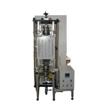
- Customer Made Versatile CVD Tube Furnace Chemical Vapor Deposition Chamber System Equipment
- Split Chamber CVD Tube Furnace with Vacuum Station Chemical Vapor Deposition System Equipment Machine
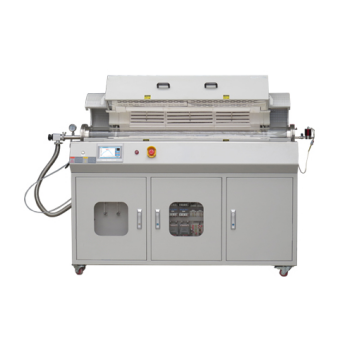
- 1200℃ Split Tube Furnace with Quartz Tube Laboratory Tubular Furnace
- Vertical Laboratory Quartz Tube Furnace Tubular Furnace
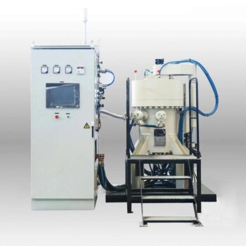
- Vacuum Hot Press Furnace Heated Vacuum Press Machine Tube Furnace
People Also Ask
- Are all lab grown diamonds CVD? Understanding the Two Main Methods
- Why are carbon nanotubes important in industry? Unlocking Next-Generation Material Performance
- What are the methods of producing CNT? Scalable CVD vs. High-Purity Lab Techniques
- What are nanotubes drawbacks? The 4 Major Hurdles Limiting Their Real-World Use
- What is the floating catalyst method? A Guide to High-Yield CNT Production