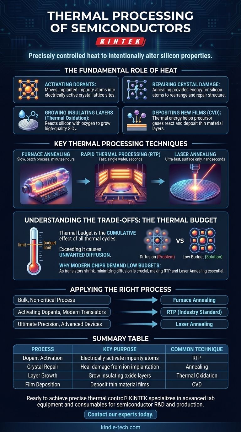
In semiconductor manufacturing, thermal processing is the practice of using precisely controlled heat to intentionally alter the physical and chemical properties of a silicon wafer. These processes are not about simply warming the material; they are fundamental, high-energy steps that activate materials, repair crystal structures, and grow or deposit essential layers, turning a simple silicon disc into a complex integrated circuit.
The core purpose of thermal processing is to provide the necessary energy—the "thermal budget"—to drive specific atomic-level changes. The central challenge is achieving these desired changes without causing unwanted side effects, like the diffusion of materials, which becomes more critical as transistors shrink.
The Fundamental Role of Heat in Chipmaking
Heat is one of the most powerful tools in semiconductor fabrication. At room temperature, the atoms in a silicon crystal are relatively stable. Applying thermal energy allows engineers to overcome this stability and force specific, desirable reactions to occur on and within the wafer.
Activating Dopants
To control the flow of electricity, pure silicon is "doped" with impurity atoms like boron or phosphorus through a process called ion implantation. However, these implanted atoms are initially not in the right positions within the silicon crystal lattice to be electrically active. Thermal processing provides the energy needed for these dopant atoms to move into the correct lattice sites, a critical step known as dopant activation.
Repairing Crystal Damage
The process of ion implantation is physically violent at an atomic scale. It bombards the wafer with high-energy ions, which severely damages the perfect, ordered structure of the silicon crystal. This damage must be repaired. Annealing, a key thermal process, provides the energy for the silicon atoms to rearrange themselves back into their pristine crystalline structure, ensuring electrons can flow smoothly.
Growing Insulating Layers
One of the most important components in a transistor is the gate oxide, a thin, perfect insulating layer. This is typically created using thermal oxidation, where the silicon wafer is heated in an oxygen-rich environment. The heat drives a chemical reaction between the silicon and oxygen to grow an exceptionally high-quality layer of silicon dioxide (SiO₂).
Depositing New Films
Many other material layers are added to a chip during manufacturing. In processes like Chemical Vapor Deposition (CVD), thermal energy is used to help precursor gases react and deposit thin films of insulating or conductive materials onto the wafer's surface with high precision.
Key Thermal Processing Techniques
Different steps in chip fabrication have different requirements for temperature and time. Consequently, several distinct methods have been developed to manage the application of heat.
Furnace Annealing
This is the traditional method, where a batch of 25 to 200 wafers is loaded into a quartz tube and heated slowly in a furnace. While it is efficient for processing many wafers at once, the heating and cooling cycles are very slow (minutes to hours). This makes it suitable for non-critical steps like initial oxide growth but problematic for advanced devices.
Rapid Thermal Processing (RTP)
RTP is the dominant technique for modern semiconductor manufacturing. A single wafer is heated very quickly (in seconds) to extremely high temperatures using high-intensity lamps. By precisely controlling the heat for a very short duration, RTP can achieve the necessary activation and damage repair without the negative side effects of prolonged heat exposure.
Laser Annealing
For the most advanced chips, even the seconds-long duration of RTP can be too long. Laser annealing provides an even more precise solution by using a laser to heat only the top few nanometers of the wafer's surface. This delivers the required energy exactly where it's needed without disturbing the delicate structures underneath.
Understanding the Trade-offs: The Thermal Budget
The primary challenge in all thermal processing is managing the thermal budget. This concept is central to understanding why modern techniques like RTP were developed.
What is the Thermal Budget?
The thermal budget is the cumulative effect of all the thermal cycles (temperature and duration) a wafer is exposed to during manufacturing. Every heating step "spends" some of this budget. Like a financial budget, once it's used up, you can't get it back.
The Problem of Unwanted Diffusion
The main consequence of exceeding the thermal budget is diffusion. When dopant atoms are exposed to heat for too long, they begin to move or "diffuse" away from their intended positions. This blurring of carefully defined regions can ruin a transistor's performance, causing short circuits or device failure.
Why Modern Chips Demand Low Thermal Budgets
As transistors shrink to the nanometer scale, the doped regions are placed incredibly close together. Any diffusion is catastrophic. The goal of modern thermal processing is to get the heat in and out as fast as possible—achieving activation and repair while minimizing diffusion. This is why RTP and laser annealing are essential for manufacturing today's high-performance chips.
Applying the Right Thermal Process
Choosing the correct thermal technique is about matching the tool to the specific requirement of the fabrication step, with the thermal budget as the primary constraint.
- If your primary focus is a bulk, non-critical process: Traditional furnace annealing is a cost-effective choice for steps where slow heating and potential diffusion are not a concern.
- If your primary focus is activating dopants in modern transistors: Rapid Thermal Processing (RTP) is the industry standard, providing the necessary high temperatures for short durations to minimize the thermal budget.
- If your primary focus is ultimate precision on the most advanced devices: Laser annealing offers localized, near-instantaneous heating to activate surface layers without affecting the complex structures beneath.
Ultimately, thermal processing is the art of using controlled energy to achieve atomic-level precision across a silicon wafer.
Summary Table:
| Process | Key Purpose | Common Technique |
|---|---|---|
| Dopant Activation | Electrically activate impurity atoms | Rapid Thermal Processing (RTP) |
| Crystal Repair | Heal damage from ion implantation | Annealing |
| Layer Growth | Grow insulating oxide layers | Thermal Oxidation |
| Film Deposition | Deposit thin material films | Chemical Vapor Deposition (CVD) |
Ready to achieve precise thermal control in your lab?
KINTEK specializes in the advanced lab equipment and consumables needed for semiconductor R&D and production. Our thermal processing solutions help you manage the critical thermal budget for next-generation chips.
Contact our experts today to discuss your specific application needs.
Visual Guide
Related Products
- Laboratory Rapid Thermal Processing (RTP) Quartz Tube Furnace
- Multi Heating Zones CVD Tube Furnace Machine Chemical Vapor Deposition Chamber System Equipment
- Spark Plasma Sintering Furnace SPS Furnace
- Chemical Vapor Deposition CVD Equipment System Chamber Slide PECVD Tube Furnace with Liquid Gasifier PECVD Machine
- Graphite Vacuum Furnace High Thermal Conductivity Film Graphitization Furnace
People Also Ask
- What is the maximum temperature for a quartz tube furnace? Key Limits for Safe & Efficient Operation
- What is the temperature of a quartz tube furnace? Master the Limits for Safe, High-Temp Operation
- Why use a quartz tube furnace for metal alloy nanoparticles? Essential for High Purity & Preventing Oxidation
- What experimental conditions does a quartz tube furnace provide when evaluating CO oxidation reaction performance? Ensure Precision
- What are the advantages of using an electric heating furnace with a quartz tube for liquid bismuth corrosion control?