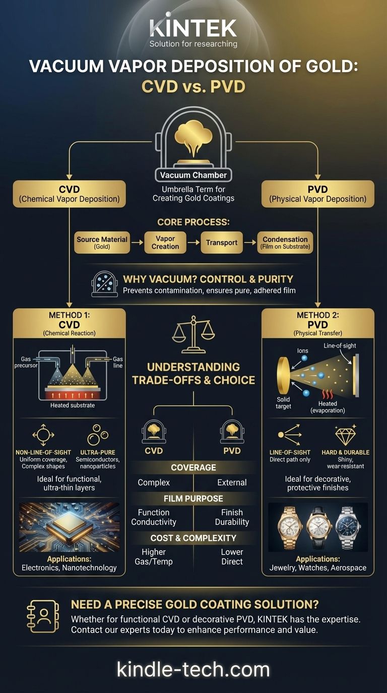
In short, vacuum vapor deposition of gold is a high-tech process where a thin, precise layer of gold is applied to a surface inside a vacuum chamber. This isn't a single technique but a category of methods, most commonly Chemical Vapor Deposition (CVD) or Physical Vapor Deposition (PVD), used to impart gold's properties—like conductivity or appearance—onto another material without making the entire object out of solid gold.
The central concept to grasp is that "vacuum vapor deposition" is an umbrella term for processes that turn gold into a vapor to create a coating. The specific method used, such as a chemical reaction (CVD) or physical transfer (PVD), is chosen based on whether the goal is functional purity for electronics or a durable, decorative finish.
Deconstructing the Core Process
At its heart, all vacuum vapor deposition involves three fundamental stages: creating a vapor from the source material (in this case, gold), transporting that vapor, and having it condense or react to form a solid film on a target object, known as the substrate.
The Critical Role of the Vacuum
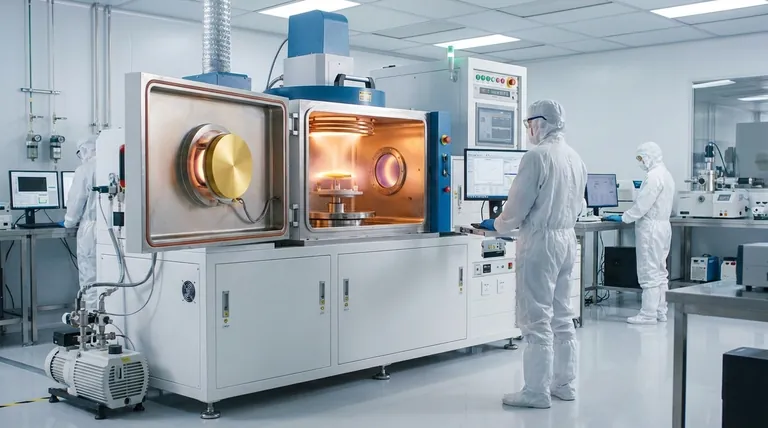
The entire process is performed in a vacuum for a simple reason: control. Removing air and other atmospheric gases prevents contamination from unwanted particles and chemical reactions, ensuring the resulting gold film is exceptionally pure and adheres properly to the surface.
The Two Primary Methods
While there are many variations, the vast majority of commercial gold vapor deposition falls into two categories. The key difference between them is how the gold vapor is created and deposited.
- Chemical Vapor Deposition (CVD): Uses a chemical reaction.
- Physical Vapor Deposition (PVD): Uses a physical mechanism, like evaporation or sputtering.
Method 1: Chemical Vapor Deposition (CVD)
CVD is a sophisticated process that builds the gold film through a controlled chemical reaction directly on the substrate's surface.
The Core CVD Process
A substrate is placed in a reaction chamber filled with a gas containing gold chemical compounds (known as precursors). When these gaseous precursors make contact with the heated substrate, they react and decompose, leaving behind a pure, solid gold film.
Key Characteristics of CVD
Because the deposition happens from a gas that fills the entire chamber, CVD has a unique advantage: it is non-line-of-sight. This allows it to coat complex, intricate shapes and even internal surfaces with a perfectly uniform layer. The process offers exceptional control over film purity, density, and thickness.
Common Applications
CVD is essential for applications demanding ultra-pure, ultra-thin functional layers. It is frequently used to deposit thin films on semiconductors for electronics, to create nanoparticles and nanowires, and to produce highly specific layers for advanced materials science.
Method 2: Physical Vapor Deposition (PVD)
PVD is the more common method for applying gold for decorative and protective purposes. Instead of a chemical reaction, it physically transfers gold from a solid source to the substrate.
The Core PVD Process
Inside the vacuum chamber, a solid gold target is bombarded with high-energy ions (sputtering) or heated until it evaporates. This creates a gold vapor that travels in a straight line and condenses onto the substrate, forming a thin, hard, and durable coating.
Key Characteristics of PVD
PVD is a line-of-sight process, meaning it can only coat surfaces that are directly exposed to the vapor source. The resulting gold film is known for being extremely smooth, shiny, and wear-resistant, making it ideal for products that need both beauty and durability.
Common Applications
PVD is the go-to method for the gold coatings you see on everyday luxury items. It is used extensively for jewelry and watches to provide a brilliant finish and is also applied in the aerospace industry for components that require a durable, reflective surface.
Understanding the Trade-offs
Choosing between CVD and PVD depends entirely on the end goal. Neither is universally "better"; they are simply different tools for different jobs.
Coverage vs. Directionality
CVD excels at providing uniform coverage on parts with complex geometries due to its non-line-of-sight nature. PVD is line-of-sight, making it perfect for external surfaces but less suitable for coating inside cavities or complex internal structures.
Film Purpose: Function vs. Finish
CVD is typically chosen when the purity and electrical properties of the gold film are paramount, as in microelectronics. PVD is the standard when the goal is a hard, wear-resistant, and aesthetically pleasing surface finish.
Process Complexity and Cost
Generally, CVD setups can be more complex due to the management of reactive gases and higher temperatures. PVD can often be a more direct and cost-effective process, especially for creating decorative coatings on a large scale.
Making the Right Choice for Your Application
To determine the right method, you must first define your primary objective.
- If your primary focus is high-purity electrical conductivity for circuits or semiconductors: CVD is the superior choice due to its precise control over film composition.
- If your primary focus is a durable, brilliant, and wear-resistant decorative finish for jewelry or watches: PVD is the industry-standard method.
- If your primary focus is uniform coating on a highly complex part with internal surfaces: CVD's non-line-of-sight nature makes it the only viable option.
Ultimately, understanding the fundamental difference between a chemical reaction and a physical transfer is the key to selecting the right technology for your goal.
Summary Table:
| Method | Key Process | Best For | Key Characteristic |
|---|---|---|---|
| Chemical Vapor Deposition (CVD) | Chemical reaction of gases on a heated substrate | High-purity electronics, semiconductors, complex parts | Non-line-of-sight, uniform coating |
| Physical Vapor Deposition (PVD) | Physical transfer via sputtering or evaporation | Decorative finishes, jewelry, wear-resistant coatings | Line-of-sight, hard and durable finish |
Need a precise and durable gold coating solution?
Whether your project requires the ultra-pure functional layers of CVD for semiconductors or the brilliant, hard-wearing decorative finish of PVD for luxury goods, KINTEK has the expertise and equipment to meet your specific laboratory and production needs.
Contact our experts today to discuss how our vacuum deposition solutions can enhance your product's performance, value, and durability.
Visual Guide
Related Products
- CVD Diamond Dressing Tools for Precision Applications
- Microwave Plasma Chemical Vapor Deposition MPCVD Machine System Reactor for Lab and Diamond Growth
- HFCVD Machine System Equipment for Drawing Die Nano-Diamond Coating
- Chemical Vapor Deposition CVD Equipment System Chamber Slide PECVD Tube Furnace with Liquid Gasifier PECVD Machine
- Electron Beam Evaporation Coating Gold Plating Tungsten Molybdenum Crucible for Evaporation
People Also Ask
- What color diamonds are CVD? Understanding the Process from Brown Tint to Colorless Beauty
- Can CVD diamonds change color? No, their color is permanent and stable.
- How long does it take to make synthetic diamonds? Discover the 6-8 Week Science Behind Lab-Grown Gems
- What are the raw materials for CVD diamonds? A seed, a gas, and the science of crystal growth.
- What is CVD diamond? The Ultimate Guide to Lab-Grown Diamonds and Their Uses


