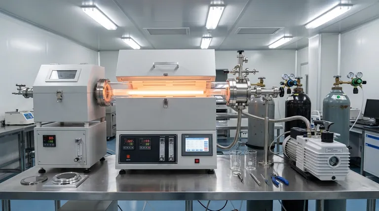
At its core, vapor deposition is a family of processes used to apply an ultra-thin layer of material—often just a few atoms or molecules thick—onto a surface. This is accomplished by converting a solid or liquid coating material into a gas or vapor within a vacuum chamber, allowing it to travel and then solidify onto a target object, known as the substrate.
Vapor deposition is not a single technique but a fundamental principle: turning a material into a vapor so it can be precisely reassembled as a solid thin film on a new surface. The crucial difference lies in how that reassembly happens—either through a physical process (condensation) or a chemical one (reaction).
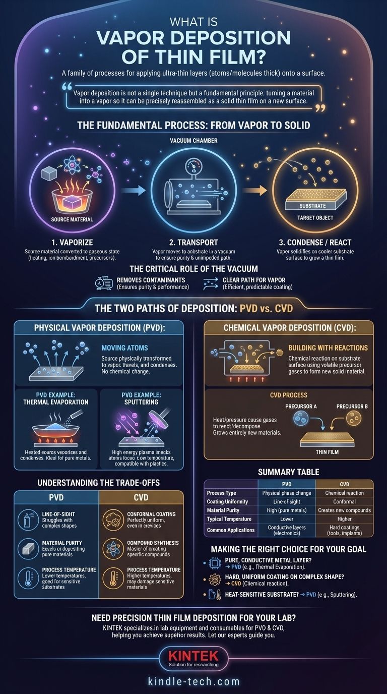
The Fundamental Process: From Vapor to Solid
Vapor deposition may sound complex, but the underlying principle follows a logical, three-step sequence. It is a highly controlled method for building materials from the ground up.
The Three Core Steps
The entire process hinges on three distinct phases. First, a source material is converted into a gaseous state, creating a vapor. This is done through heating, bombardment with ions, or introducing reactive precursor gases.
Second, this vapor is transported from the source to the substrate. This almost always occurs within a vacuum to ensure purity and prevent the vapor atoms from colliding with air molecules.
Third, the vapor condenses or reacts on the cooler substrate surface, growing into a solid, uniform thin film. Think of it like steam from a hot shower condensing into a layer of water on a cold mirror, but on a highly engineered, atomic scale.
The Critical Role of the Vacuum
A vacuum environment is non-negotiable for high-quality vapor deposition. It serves two primary functions.
First, it removes air and other contaminants that could otherwise get trapped in the thin film, compromising its purity and performance.
Second, it creates a clear, unimpeded path for the vaporized atoms to travel from their source to the substrate, ensuring an efficient and predictable coating process.
The Two Paths of Deposition: PVD vs. CVD
While the goal is the same, there are two main categories of vapor deposition, distinguished by how the vapor becomes a solid film: Physical Vapor Deposition (PVD) and Chemical Vapor Deposition (CVD).
Physical Vapor Deposition (PVD): Moving Atoms
In PVD, the source material is physically transformed into a vapor, travels to the substrate, and condenses back into a solid. No chemical change occurs in the material itself. It is purely a phase change from solid to gas and back to solid.
PVD Example: Thermal Evaporation
One of the most straightforward PVD methods is thermal evaporation. The source material is heated in a vacuum—often by a tungsten element—until it vaporizes. This vapor then travels and condenses on the cooler substrate, forming the film. This is ideal for depositing pure materials like metals for conductive layers in solar cells or OLED displays.
PVD Example: Sputtering
Sputtering is a different physical approach. Instead of heat, it uses kinetic energy. Inside the vacuum, a high-energy plasma (typically an inert gas like argon) is directed at the source material, or "target." The plasma ions act like a subatomic sandblaster, knocking atoms loose from the target, which then fly off and deposit onto the substrate.
Chemical Vapor Deposition (CVD): Building with Reactions
Unlike PVD, Chemical Vapor Deposition involves a chemical reaction directly on the substrate's surface. In this process, one or more volatile precursor gases are introduced into a reaction chamber containing the substrate.
The heat and pressure conditions in the chamber cause these gases to react with each other or decompose on the substrate, forming an entirely new solid material as the thin film. The film is literally "grown" through a chemical synthesis.
Understanding the Trade-offs
Choosing between PVD and CVD depends entirely on the material, the shape of the object being coated, and the desired properties of the final film.
Conformal Coating vs. Line-of-Sight
PVD is largely a line-of-sight process. The vaporized atoms travel in straight lines, meaning they coat surfaces directly facing the source very well but struggle to cover complex, three-dimensional shapes uniformly.
CVD, however, relies on a gas that can flow around an object. This allows it to create highly conformal coatings that are perfectly uniform, even inside crevices and on complex geometries.
Material Purity vs. Compound Synthesis
PVD excels at depositing very pure materials. Since you are just evaporating and re-condensing the source material (e.g., pure aluminum), the final film maintains that purity.
CVD is the master of compound synthesis. It is used to create specific, durable compounds like titanium nitride (for tool coatings) or silicon dioxide (for electronics), which would be difficult or impossible to deposit with PVD.
Process Temperature
Process temperature is another key differentiator. Many CVD processes require very high temperatures to drive the necessary chemical reactions, which can limit the types of substrates that can be coated without being damaged.
While some PVD methods use heat, others like sputtering can be performed at much lower temperatures, making them compatible with more sensitive materials, including plastics.
Making the Right Choice for Your Goal
To select the correct approach, you must first define your objective.
- If your primary focus is depositing a pure, conductive metal layer (e.g., for electronics): Physical Vapor Deposition (PVD) methods like thermal evaporation are often the most direct and effective.
- If your primary focus is creating a hard, protective, and uniform coating on a complex shape (e.g., a tool or medical implant): Chemical Vapor Deposition (CVD) is likely the superior choice due to its chemical reaction process and conformal coverage.
- If your project involves a heat-sensitive substrate that cannot withstand high temperatures: A lower-temperature PVD method like sputtering often provides a significant advantage over traditional CVD.
Understanding these foundational principles empowers you to engineer materials with precision, building the functional surfaces that drive modern technology.
Summary Table:
| Feature | PVD (Physical Vapor Deposition) | CVD (Chemical Vapor Deposition) |
|---|---|---|
| Process Type | Physical phase change (evaporation/sputtering) | Chemical reaction on substrate surface |
| Coating Uniformity | Line-of-sight (less uniform on complex shapes) | Conformal (excellent for 3D shapes) |
| Material Purity | High (pure metals) | Creates new compounds (e.g., titanium nitride) |
| Typical Temperature | Lower (suitable for heat-sensitive substrates) | Higher (may damage sensitive materials) |
| Common Applications | Conductive layers in electronics, solar cells | Hard coatings for tools, medical implants |
Need Precision Thin Film Deposition for Your Lab?
Whether you're developing advanced electronics, durable tool coatings, or medical device surfaces, choosing the right vapor deposition method is critical. KINTEK specializes in lab equipment and consumables for both PVD and CVD processes, helping you achieve superior thin film results with precision and reliability.
Let our experts guide you to the optimal solution for your specific application.
Contact us today to discuss your project requirements!
Visual Guide
Related Products
- Chemical Vapor Deposition CVD Equipment System Chamber Slide PECVD Tube Furnace with Liquid Gasifier PECVD Machine
- RF PECVD System Radio Frequency Plasma-Enhanced Chemical Vapor Deposition RF PECVD
- Microwave Plasma Chemical Vapor Deposition MPCVD Machine System Reactor for Lab and Diamond Growth
- 915MHz MPCVD Diamond Machine Microwave Plasma Chemical Vapor Deposition System Reactor
- Customer Made Versatile CVD Tube Furnace Chemical Vapor Deposition Chamber System Equipment
People Also Ask
- What are the core advantages of PE-CVD in OLED encapsulation? Protect Sensitive Layers with Low-Temp Film Deposition
- What are the advantages of chemical vapor deposition? Achieve Superior Thin Films for Your Lab
- What is the chemical vapor deposition growth process? Build Superior Thin Films from the Atom Up
- What types of substrates are used in CVD to facilitate graphene films? Optimize Graphene Growth with the Right Catalyst
- What is plasma enhanced chemical vapor deposition PECVD equipment? A Guide to Low-Temperature Thin Film Deposition


