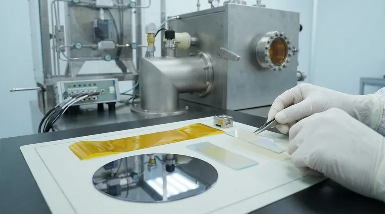
At its core, a thin film can be deposited on a wide range of materials, including silicon wafers, glass, plastics, and metals. The specific material chosen is not arbitrary; it is a critical engineering decision dictated by the deposition method and the final application of the component.
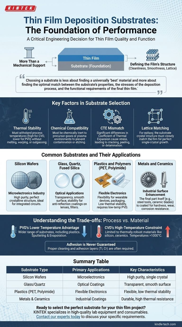
Choosing a substrate is less about finding a universally "best" material and more about finding the optimal match between the substrate's properties, the stresses of the deposition process, and the functional requirements of the final thin film.
The Role of the Substrate in Film Quality
The substrate is the foundation upon which your thin film is built. Its properties directly influence the quality, adhesion, and ultimate performance of the film itself.
More Than Just a Mechanical Support
While the substrate provides the physical surface for deposition, its role is far more active than that of a simple base layer. It is an integral part of the final electronic, optical, or mechanical system.
Defining the Film's Structure
The substrate's surface condition—its cleanliness, smoothness, and even its crystalline structure—can determine how the film atoms or molecules arrange themselves. A rough or contaminated surface can lead to poor adhesion and defects in the film.
Key Factors in Substrate Selection
Selecting the correct substrate requires a systematic evaluation of its properties against the demands of both the deposition process and the end-use application.
Thermal Stability
Deposition processes often involve significant heat. Physical Vapor Deposition (PVD) methods are generally cooler, while Chemical Vapor Deposition (CVD) often requires high temperatures to drive chemical reactions. The substrate must maintain its structural integrity without melting, warping, or outgassing at these process temperatures.
Chemical Compatibility
The substrate must be chemically inert to the precursor gases (in CVD) or plasma environment. Unwanted chemical reactions between the substrate and the deposition environment can contaminate the film or etch the substrate surface, compromising the entire process.
Coefficient of Thermal Expansion (CTE)
Every material expands and contracts with temperature. If the substrate and the thin film have a significant CTE mismatch, immense stress will build up as the component cools down from the deposition temperature. This stress can cause the film to crack, peel, or delaminate.
Lattice Matching
For advanced applications like semiconductor epitaxy, the goal is to grow a perfect, single-crystal thin film. This requires the substrate to have a crystal lattice structure that is very closely matched to that of the film material, providing a template for growth.
Common Substrates and Their Applications
The choice of substrate is directly tied to the industry and application.
Silicon Wafers
The undisputed standard for the microelectronics industry. Silicon's high purity, perfect crystalline structure, and well-understood properties make it the ideal foundation for building integrated circuits.
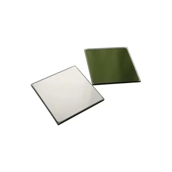
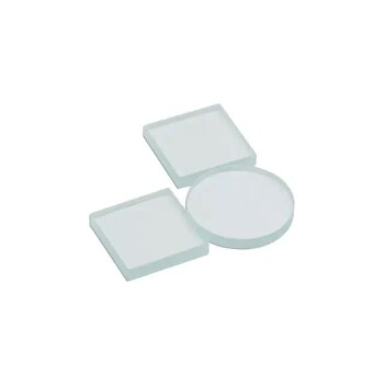
Glass, Quartz, and Fused Silica
These materials are chosen for optical applications. Their transparency, smooth surface finish, and stability make them perfect for anti-reflection coatings on lenses, filters, and mirrors.
Plastics and Polymers
Substrates like PET (polyethylene terephthalate) and polyimide (Kapton) are used for flexible electronics, wearable devices, and food packaging. Their flexibility is key, but they typically have low thermal stability, restricting their use to low-temperature deposition methods.
Metals and Ceramics
For industrial applications, the substrate is often the final part itself. A steel tool bit, an aluminum automotive part, or a ceramic turbine blade can be coated to enhance hardness, wear resistance, or corrosion protection.
Understanding the Trade-offs: Process vs. Material
No choice is without compromise. The interplay between the deposition method and the substrate material is a primary source of constraints.
PVD's Lower Temperature Advantage
Processes like sputtering and evaporation generally operate at lower temperatures. This opens up a wider range of possible substrates, including many plastics and polymers that would be destroyed by high-heat methods.
CVD's High-Temperature Constraint
Many CVD processes require temperatures exceeding several hundred or even a thousand degrees Celsius. This immediately disqualifies most polymers and many low-melting-point metals, restricting the choice to thermally robust materials like silicon, quartz, or ceramics.
Adhesion Is Never Guaranteed
Simply placing a material in a deposition chamber does not ensure the film will stick. Proper surface cleaning and preparation are critical. In some cases, a thin "adhesion layer" of a material like titanium or chromium must be deposited first to act as a glue between the substrate and the functional film.
Selecting the Right Substrate for Your Goal
Your final objective dictates your starting material.
- If your primary focus is microelectronics: Your choice is almost always a high-purity silicon wafer for its perfect crystal structure and compatibility with fabrication processes.
- If your primary focus is an optical coating: You will use a high-quality glass, quartz, or fused silica with an exceptionally smooth surface.
- If your primary focus is a flexible device: You must select a polymer substrate like PET or polyimide and use a low-temperature deposition process.
- If your primary focus is industrial surface enhancement: The substrate is the component you need to improve, often a metal or ceramic part, and the deposition process is chosen to be compatible with it.
Ultimately, the substrate is not an afterthought but the first strategic decision in any successful thin film application.
Summary Table:
| Substrate Type | Primary Applications | Key Characteristics |
|---|---|---|
| Silicon Wafers | Microelectronics | High purity, single crystal |
| Glass/Quartz | Optical Coatings | Transparent, smooth surface |
| Plastics (PET, Polyimide) | Flexible Electronics | Flexible, low thermal stability |
| Metals & Ceramics | Industrial Coatings | Durable, high thermal resistance |
Ready to select the perfect substrate for your thin film project? KINTEK specializes in providing high-quality lab equipment and consumables for all your deposition needs. Whether you're working with silicon wafers, glass, or specialized polymers, our expertise ensures you have the right foundation for success. Contact our experts today to discuss your specific requirements and discover how we can support your laboratory's thin film applications.
Visual Guide
Related Products
- Aluminized Ceramic Evaporation Boat for Thin Film Deposition
- Tungsten Evaporation Boat for Thin Film Deposition
- Molybdenum Tungsten Tantalum Evaporation Boat for High Temperature Applications
- Electron Beam Evaporation Coating Oxygen-Free Copper Crucible and Evaporation Boat
- MgF2 Magnesium Fluoride Crystal Substrate Window for Optical Applications
People Also Ask
- What are thin films deposited by evaporation? A Guide to High-Purity Coating
- What is thin film deposition? Unlock Advanced Surface Engineering for Your Materials
- What is the chemical method for thin film deposition? Build Films from the Molecular Level Up
- Why is an alumina boat and Ti3AlC2 powder bed necessary for Ti2AlC sintering? Protect MAX Phase Purity
- What is the widely used boat made of in thermal evaporation? Choosing the Right Material for High-Purity Deposition