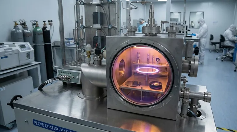
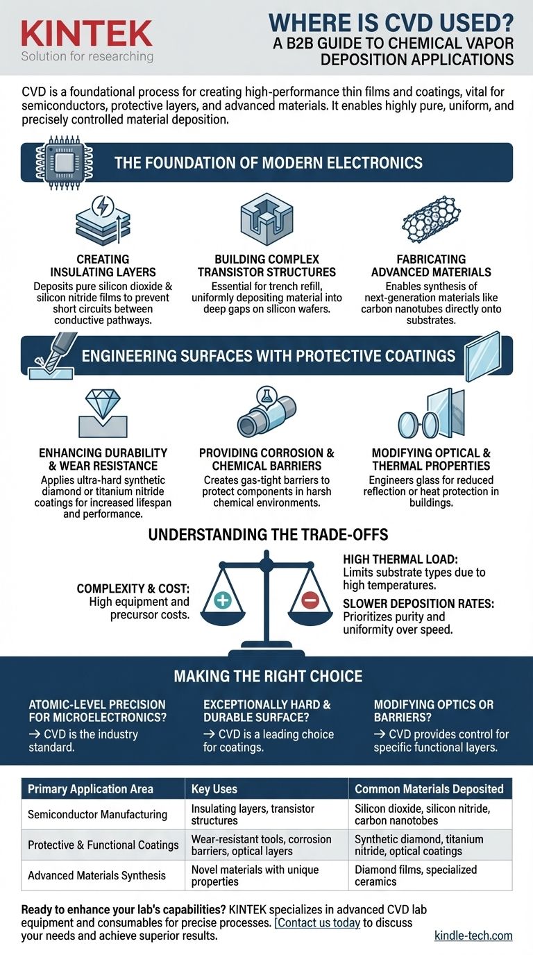
At its core, Chemical Vapor Deposition (CVD) is a foundational manufacturing process used to create high-performance thin films and coatings. It is most prominently used in the semiconductor industry for manufacturing microchips, but its applications extend to creating durable protective coatings for tools and glass, advanced optical layers, and even synthesizing novel materials like synthetic diamonds.
Chemical Vapor Deposition isn't just one application; it's a versatile platform technology. Its primary value lies in its ability to deposit highly pure, uniform, and precisely controlled layers of material onto a substrate, enabling properties that are impossible to achieve through other means.
The Foundation of Modern Electronics
The semiconductor industry relies heavily on CVD to build the microscopic, multi-layered structures that make up integrated circuits. Without it, modern computing would not exist.
Creating Insulating and Dielectric Layers
In a microchip, billions of transistors are packed together. CVD is used to deposit extremely thin, pure layers of insulating materials like silicon dioxide and silicon nitride. These films prevent electrical "short circuits" between the different conductive pathways.
Building Complex Transistor Structures
Modern chip designs involve intricate three-dimensional features. CVD is essential for processes like trench refill, where it uniformly deposits material into deep, narrow gaps on a silicon wafer, forming critical parts of the transistor architecture.
Fabricating Advanced Materials
The precision of CVD allows for the synthesis of next-generation materials directly onto a substrate. A key example is the controlled growth of carbon nanotubes, which have unique electrical and mechanical properties with potential for future electronics.
Engineering Surfaces with Protective Coatings
Beyond electronics, CVD is a dominant method for fundamentally changing the surface properties of a material, making it stronger, more resilient, or functionally different.
Enhancing Durability and Wear Resistance
CVD is used to apply ultra-hard coatings, such as synthetic diamond or titanium nitride, onto cutting tools, drill bits, and industrial components. This drastically increases their lifespan and performance by providing exceptional wear resistance.
Providing Corrosion and Chemical Barriers
A thin, dense layer deposited by CVD can create a completely gas-tight barrier. This protects sensitive components from corrosion and is used in the chemical industry to line reactors or pipes, preventing degradation from harsh substances.
Modifying Optical and Thermal Properties
The properties of glass can be precisely engineered using CVD. This includes applying optical coatings to lenses to reduce reflection or depositing heat-protection layers on architectural glass to improve energy efficiency in buildings.
Understanding the Trade-offs
While incredibly powerful, CVD is a specialized process with inherent complexities and limitations that make it suitable for high-value applications.
Process Complexity and Cost
CVD requires a vacuum chamber, high temperatures, and a complex system for controlling the flow of reactive gases. This equipment represents a significant capital investment, and the precursor gases themselves can be expensive and hazardous.
High Thermal Load
The process typically requires heating the substrate to high temperatures to drive the chemical reaction. This can limit the types of materials that can be coated, as some substrates may not be able to withstand the heat without deforming or melting.
Slower Deposition Rates
Compared to some other methods like Physical Vapor Deposition (PVD), CVD can have a slower rate of material deposition. It is chosen when the purity, density, and uniformity of the film are more critical than raw speed.
Making the Right Choice for Your Application
The decision to use CVD is driven by the need for performance that justifies the process complexity.
- If your primary focus is atomic-level precision for microelectronics: CVD is the non-negotiable industry standard for creating insulating films and building transistors.
- If your primary focus is creating an exceptionally hard and durable surface: CVD is a leading choice for coating tools and high-wear components with materials like synthetic diamond.
- If your primary focus is modifying surface properties for optics or barriers: CVD provides the control needed to create highly specific functional layers for glass, chemical processing, and photovoltaics.
Ultimately, Chemical Vapor Deposition is the critical enabling technology behind many of the highest-performing materials that define our modern world.
Summary Table:
| Primary Application Area | Key Uses | Common Materials Deposited |
|---|---|---|
| Semiconductor Manufacturing | Insulating layers, transistor structures, advanced materials | Silicon dioxide, silicon nitride, carbon nanotubes |
| Protective & Functional Coatings | Wear-resistant tools, corrosion barriers, optical layers | Synthetic diamond, titanium nitride, optical coatings |
| Advanced Materials Synthesis | Creating novel materials with unique properties | Diamond films, specialized ceramics |
Ready to enhance your lab's capabilities with high-performance thin films? KINTEK specializes in providing advanced lab equipment and consumables tailored for precise Chemical Vapor Deposition (CVD) processes. Whether you're in semiconductor research, materials science, or surface engineering, our solutions deliver the purity, uniformity, and control your work demands. Contact us today to discuss how we can support your specific laboratory needs and help you achieve superior results.
Visual Guide
Related Products
- CVD Diamond Dressing Tools for Precision Applications
- Multi Heating Zones CVD Tube Furnace Machine Chemical Vapor Deposition Chamber System Equipment
- CVD Diamond Domes for Industrial and Scientific Applications
- CVD Diamond for Thermal Management Applications
- Chemical Vapor Deposition CVD Equipment System Chamber Slide PECVD Tube Furnace with Liquid Gasifier PECVD Machine
People Also Ask
- What are the raw materials for CVD diamonds? A seed, a gas, and the science of crystal growth.
- How do CVD diamonds grow? A Step-by-Step Guide to Lab-Grown Diamond Creation
- What are the disadvantages of CVD diamonds? Understanding the trade-offs for your purchase.
- Does the chemical vapor deposition be used for diamonds? Yes, for Growing High-Purity Lab Diamonds
- Can CVD diamonds change color? No, their color is permanent and stable.


