The requirement for Plasma Enhanced Chemical Vapor Deposition (PECVD) in vertical graphene synthesis is driven by the need for directional control. PECVD utilizes plasma-induced electric fields to guide carbon atoms into a perpendicular orientation relative to the substrate, a feat impossible with standard thermal methods. This process lowers the reaction's activation energy, enabling the formation of high-surface-area 3D nanowall structures at lower temperatures and with greater structural precision.
PECVD is indispensable for vertical graphene nanowalls because the internal electric field of the plasma sheath provides the physical force necessary to override natural horizontal growth. This process transforms a flat material into a three-dimensional network, significantly enhancing its electrochemical and surface properties.
The Mechanism of Vertical Alignment
The Role of the Plasma Sheath
The most critical reason for using PECVD is the creation of a plasma sheath near the substrate surface. This region generates a strong electric field that is oriented perpendicular to the substrate.
This field acts as a physical guide, forcing carbon atoms to deposit and grow in a vertically oriented manner. Without this field, graphene naturally tends to grow in flat, in-plane sheets due to the preferred energy states of carbon bonding.
High-Activity Chemical Radicals
PECVD systems, including RF (Radio Frequency) and Microwave (MPECVD) variants, use high-energy plasma to dissociate source gases like methane. This dissociation creates highly reactive chemical radicals that would not exist at the same concentrations in purely thermal systems.
These radicals promote high-quality crystallization and allow for the rapid building of 3D networks. The result is a structure with extremely thin, sharp edges and a high specific surface area.
Thermal and Chemical Advantages
Lowering Reaction Activation Energy
Plasma assistance significantly lowers the activation energy required for the chemical reaction to occur. This allows the growth of graphene on copper foils or dielectric substrates at much lower temperatures than traditional CVD.
Operating at lower temperatures preserves the structural integrity of sensitive substrates. It also allows for "green" production by reducing the overall energy consumption of the manufacturing process.
Controlling the Growth Environment
A PECVD system relies on a high-performance vacuum pump system to maintain a dynamic low-pressure environment. This low pressure increases the mean free path of active particles, ensuring they reach the substrate without losing energy through collisions.
This controlled environment minimizes gas-phase side reactions. By reducing impurities and side reactions, the system ensures the purity and consistency of the resulting graphene nanowall arrays.
Understanding the Trade-offs
Equipment Complexity and Cost
While PECVD offers superior structural control, it requires a significantly higher initial investment than thermal CVD. The need for RF generators, microwave sources, and sophisticated vacuum systems increases both capital and maintenance costs.
Risk of Ion Bombardment
The high-energy environment of plasma can lead to lattice defects if the power is not precisely calibrated. Excessive ion bombardment can damage the growing graphene layers, leading to structural inconsistencies rather than the desired sharp nanowalls.
Scaling and Uniformity
Achieving uniform plasma density over large surface areas is technically challenging. While PECVD is suitable for industrial scales, maintaining the uniformity of the electric field across wide substrates requires advanced reactor designs to avoid edge effects and growth variations.
How to Apply This to Your Project
When deciding if a PECVD system is necessary for your specific application, consider your primary performance metrics.
- If your primary focus is electrochemical performance (e.g., batteries): Utilize PECVD to create 3D nanowall structures that reduce lithium-ion transport resistance and maximize surface area.
- If your primary focus is substrate protection: Choose PECVD for its low-temperature operation, which allows you to grow graphene directly on dielectric or temperature-sensitive materials without damage.
- If your primary focus is surface engineering: Use the system’s electric field control to impart superhydrophobic properties or create sharp edges for efficient sterilization applications.
By leveraging the unique physics of the plasma sheath, PECVD transforms graphene from a simple two-dimensional film into a high-performance three-dimensional architecture.
Summary Table:
| Feature | Role in Vertical Growth | Key Benefit |
|---|---|---|
| Plasma Sheath | Generates a perpendicular electric field | Forces vertical alignment of carbon atoms |
| Chemical Radicals | High-energy dissociation of source gases | Promotes rapid crystallization and sharp edges |
| Activation Energy | Lowers energy needed for chemical reactions | Enables growth at lower temperatures |
| Vacuum System | Maintains dynamic low-pressure environment | Minimizes impurities and ensures consistency |
| 3D Architecture | Transforms flat sheets into nanowall arrays | Maximizes specific surface area for batteries |
Unlock the Potential of 3D Graphene with KINTEK
Ready to achieve superior structural precision in your material research? KINTEK specializes in high-performance laboratory equipment, providing advanced PECVD, CVD, and MPCVD systems designed to give you total control over the growth environment.
Whether you are developing next-generation batteries, high-surface-area catalysts, or temperature-sensitive thin films, our range of high-temperature furnaces, vacuum systems, and electrolytic cells offers the reliability and innovation your lab demands.
Why choose KINTEK?
- Precision Engineering: Systems optimized for uniform plasma density and electric field control.
- Comprehensive Solutions: From PECVD reactors to essential consumables like crucibles and ceramics.
- Expert Support: We help you select the right tools for electrochemical performance and surface engineering.
Contact KINTEK today to optimize your synthesis process!
References
- L. Li. Advancements in anode and cathode nanomaterials for high-performance Li-ion batteries. DOI: 10.54254/2755-2721/26/20230830
This article is also based on technical information from Kintek Solution Knowledge Base .
Related Products
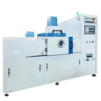
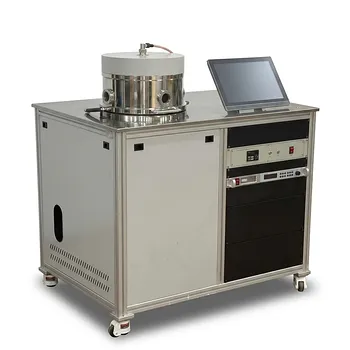
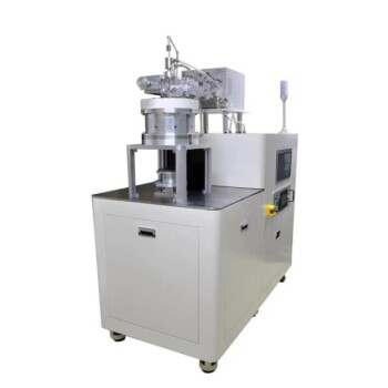
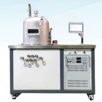
- RF PECVD System Radio Frequency Plasma-Enhanced Chemical Vapor Deposition RF PECVD
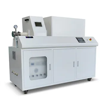
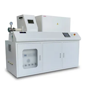
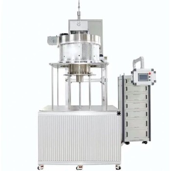
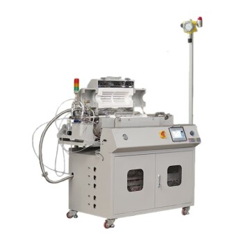
- Inclined Rotary Plasma Enhanced Chemical Vapor Deposition PECVD Equipment Tube Furnace Machine
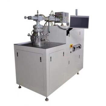
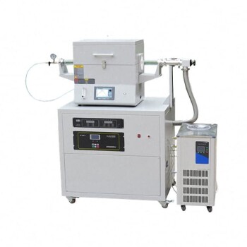
- Chemical Vapor Deposition CVD Equipment System Chamber Slide PECVD Tube Furnace with Liquid Gasifier PECVD Machine
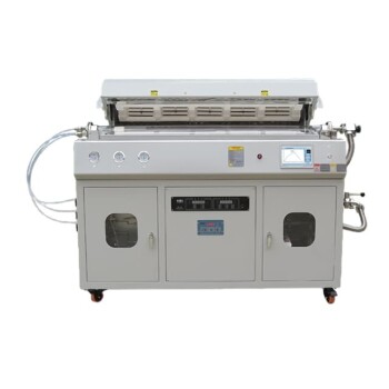
- Inclined Rotary Plasma Enhanced Chemical Vapor Deposition PECVD Equipment Tube Furnace Machine
- Microwave Plasma Chemical Vapor Deposition MPCVD Machine System Reactor for Lab and Diamond Growth
People Also Ask
- What is plasma enhanced chemical vapour deposition PECVD used for? Enable Low-Temp Thin Films for Electronics & Solar
- What is an example of PECVD? RF-PECVD for High-Quality Thin Film Deposition
- What is the role of RF-PECVD in VFG preparation? Mastering Vertical Growth and Surface Functionality
- What is plasma enhanced chemical Vapour deposition process used for fabrication of? A Guide to Low-Temperature Thin Films
- What is plasma chemical vapor deposition? A Low-Temperature Thin Film Coating Solution