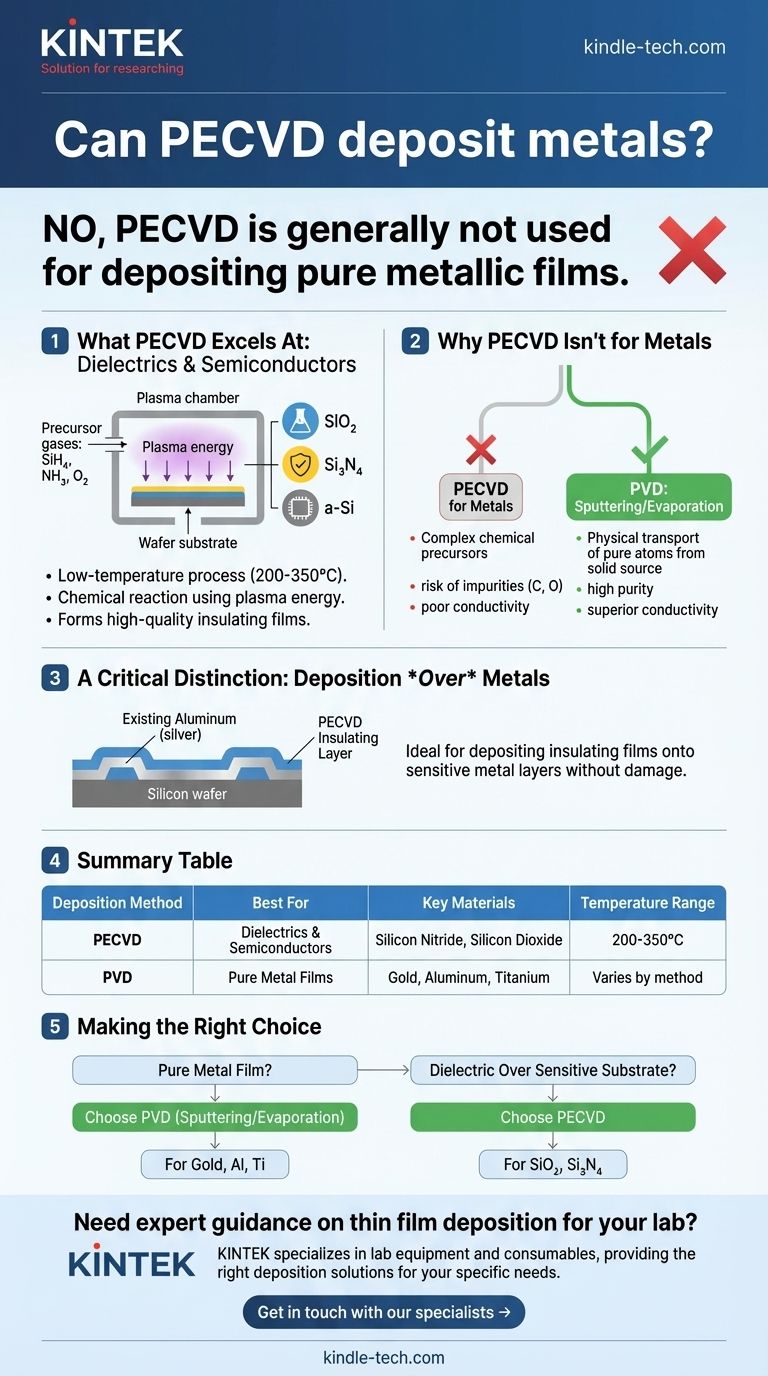
As a general rule, PECVD is not used for depositing pure metallic films. Plasma-Enhanced Chemical Vapor Deposition (PECVD) is an industry-standard process renowned for its ability to create high-quality dielectric and semiconductor thin films, such as silicon nitride and silicon dioxide, at temperatures low enough to be compatible with a wide variety of substrates.
While PECVD's low-temperature process makes it ideal for depositing insulating films onto sensitive metal layers without damaging them, it is not the standard method for depositing the metal films themselves. For that purpose, other techniques are overwhelmingly preferred.
What PECVD Excels At: Dielectrics and Semiconductors
Common PECVD Materials
The core application for PECVD is the deposition of non-metallic, inorganic films.
The process reliably produces materials like silicon dioxide (SiO₂), silicon nitride (Si₃N₄), silicon oxynitride (SiOxNy), and forms of silicon such as amorphous silicon (a-Si).
The Role of Chemical Precursors
PECVD is a chemical vapor deposition process. It works by introducing precursor gases into a chamber that chemically react to form the desired material on a substrate.
The "Plasma-Enhanced" part means that energy from a plasma is used to drive these chemical reactions. This allows the process to run at much lower temperatures (e.g., 200-350°C) than traditional thermal CVD.
Why PECVD Isn't the Go-To for Metals
The Challenge of Metal Deposition
Depositing a pure metal requires a process that transfers that metal onto the substrate without introducing contaminants.
While specialized chemical precursors for metals do exist (used in processes like MOCVD), they can be complex and risk leaving behind impurities like carbon or oxygen. This compromises the purity and conductivity of the final metallic film.
The Superiority of Physical Methods
For depositing pure metals, the industry almost universally turns to Physical Vapor Deposition (PVD) methods like sputtering or evaporation.
These techniques physically transport atoms from a solid metal source to the substrate, ensuring a high-purity film without the complexities of chemical reactions.
A Critical Distinction: Deposition Over Metals
The references highlight a key strength of PECVD: it is excellent for deposition on top of existing metal structures, such as aluminum wiring on a silicon wafer.
Because PECVD operates at low temperatures, it can deposit a high-quality insulating layer of silicon nitride over the aluminum without melting or damaging it. This is a critical step in fabricating integrated circuits.
Understanding the Trade-offs
When to Choose PECVD
PECVD is the superior choice when you need a high-quality dielectric or semiconductor film. Its primary advantages are the low process temperature and its ability to create uniform, conformal coatings over complex topographies.
When to Avoid PECVD
Do not choose PECVD when your goal is to deposit a pure metallic film. The process is not designed for this, and PVD techniques offer a more direct, effective, and higher-purity solution. Trying to adapt PECVD for this task is inefficient and yields inferior results.
Making the Right Choice for Your Goal
Selecting the correct deposition technology requires a clear understanding of your final material requirement.
- If your primary focus is depositing a pure metal film (e.g., gold, aluminum, titanium): Your best choice is a Physical Vapor Deposition (PVD) technique like sputtering or thermal evaporation.
- If your primary focus is depositing a dielectric insulating layer (e.g., SiO₂, Si₃N₄) onto a temperature-sensitive substrate, such as one with existing metal traces: PECVD is the ideal and industry-standard method.
Understanding this fundamental distinction between depositing a material and depositing onto a material is key to selecting the correct fabrication technology.
Summary Table:
| Deposition Method | Best For | Key Materials | Temperature Range |
|---|---|---|---|
| PECVD | Dielectrics & Semiconductors | Silicon Nitride, Silicon Dioxide | 200-350°C |
| PVD (Sputtering/Evaporation) | Pure Metal Films | Gold, Aluminum, Titanium | Varies by method |
Need expert guidance on thin film deposition for your lab?
KINTEK specializes in lab equipment and consumables, providing the right deposition solutions for your specific needs. Whether you require PECVD for dielectric coatings or PVD systems for metal films, our experts will help you achieve optimal results.
Contact us today to discuss your application and discover how our solutions can enhance your laboratory's capabilities.
Get in touch with our specialists →
Visual Guide
Related Products
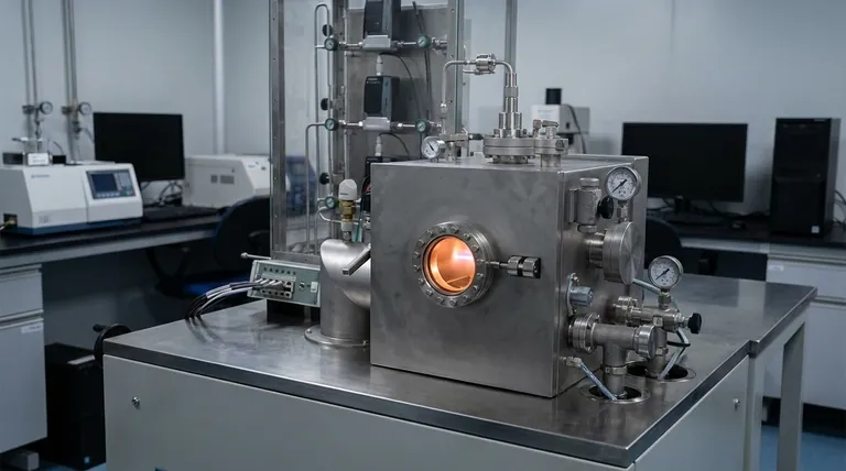
- Inclined Rotary Plasma Enhanced Chemical Vapor Deposition PECVD Equipment Tube Furnace Machine
- Chemical Vapor Deposition CVD Equipment System Chamber Slide PECVD Tube Furnace with Liquid Gasifier PECVD Machine
- Inclined Rotary Plasma Enhanced Chemical Vapor Deposition PECVD Equipment Tube Furnace Machine
- RF PECVD System Radio Frequency Plasma-Enhanced Chemical Vapor Deposition RF PECVD
- Multi Heating Zones CVD Tube Furnace Machine Chemical Vapor Deposition Chamber System Equipment
People Also Ask
- How does plasma enhanced chemical vapor deposition work? Enable Low-Temperature Thin Film Deposition
- How does PECVD facilitate Ru-C nanocomposite films? Precision Low-Temperature Thin Film Synthesis
- What is plasma enhanced chemical vapour deposition PECVD used for? Enable Low-Temp Thin Films for Electronics & Solar
- What is plasma enhanced chemical vapor deposition PECVD equipment? A Guide to Low-Temperature Thin Film Deposition
- How does PECVD equipment facilitate the directional growth of carbon nanotubes? Achieve Precision Vertical Alignment


