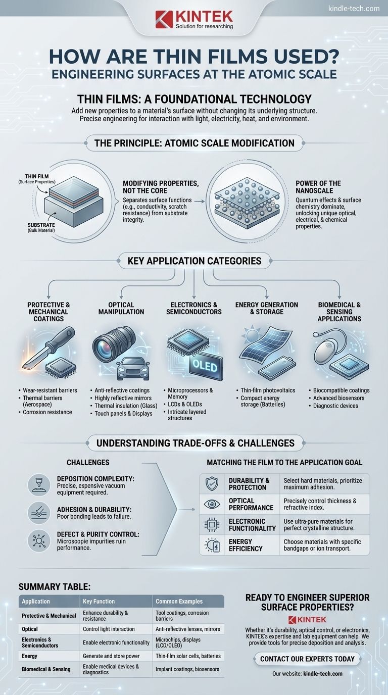
Thin films are a foundational technology used to add new properties to the surface of a material without changing its underlying structure. Their applications are incredibly diverse, ranging from protective coatings that prevent corrosion and wear on tools, to the advanced electronic layers in semiconductors, solar cells, and touch screens, and the optical films that give anti-reflective properties to glasses and lenses.
The core value of thin-film technology is its ability to precisely engineer the surface properties of an object. By applying one or more atomic-scale layers, you can control how a material interacts with light, electricity, heat, and its environment, unlocking performance that the bulk material alone could never achieve.
The Principle: Engineering Surfaces at the Atomic Scale
To understand the versatility of thin films, you must first grasp the core principles that make them so effective. It is not simply about adding a thin coat of paint; it is about manipulating matter at a near-atomic level.
Modifying Properties, Not the Core Material
The fundamental advantage of a thin film is that it separates the surface properties of an object from its bulk properties.
This allows engineers to choose a substrate material for its structural integrity, weight, or cost (like glass, plastic, or metal) and then add a thin film to provide entirely different surface functions, such as electrical conductivity or scratch resistance.
The Power of the Nanoscale
When materials are reduced to films just a few atoms thick, their behavior changes.
The high surface-to-volume ratio means that quantum effects and surface chemistry begin to dominate. This shift is what allows thin films to have unique optical, electrical, and chemical properties that are vastly different from the same material in a larger form.
Key Application Categories Explained
The use cases for thin films span nearly every modern industry. We can group them into several major categories based on their primary function.
Protective and Mechanical Coatings
This is one of the most common applications, focused on enhancing durability.
Thin films create hard, wear-resistant barriers on cutting tools and industrial components. They are also used as thermal barriers in aerospace and provide critical corrosion resistance on everything from microelectronics to architecture.
Optical Manipulation
Thin films are essential for controlling the flow of light.
They are used to create anti-reflective coatings on ophthalmic lenses and camera optics, produce highly reflective mirrors, provide thermal insulation on architectural glass, and enable touch panels and head-up displays in vehicles.
Electronics and Semiconductors
The entire digital world is built upon thin-film technology.
Thin films are used to deposit the intricate, layered structures that form microprocessors, memory chips, and other semiconductor devices. They are also the active components in Light Crystal Displays (LCDs) and Organic Light Emitting Diodes (OLEDs).
Energy Generation and Storage
Thin films are crucial for advancing clean energy technology.
Thin-film photovoltaic cells are a lightweight and flexible alternative to traditional silicon solar panels. Similarly, thin-film batteries offer new possibilities for compact energy storage in portable electronics and other devices.
Biomedical and Sensing Applications
The precision of thin films makes them ideal for sensitive medical devices.
They are used to create biocompatible coatings on implants and are the basis for advanced biosensors and plasmonic devices used in diagnostics and research.
Understanding the Trade-offs and Challenges
While incredibly powerful, the application of thin films is not without its challenges. The process requires precision and a deep understanding of material science.
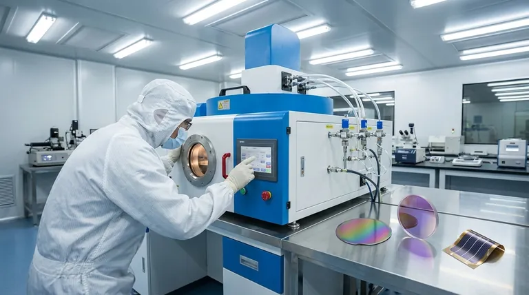
Deposition Complexity
Applying a uniform film that is only a few atoms thick is a highly technical process.
Methods like chemical or physical vapor deposition require specialized, expensive vacuum equipment and precise control over temperature, pressure, and source materials.
Adhesion and Durability
A thin film is only effective if it remains perfectly bonded to the underlying material.
Poor adhesion can cause the film to peel, crack, or flake, completely negating its benefits. Ensuring a strong, lasting bond between the film and the substrate is a critical engineering challenge.
Defect and Purity Control
In applications like semiconductors or optical coatings, even a microscopic defect or impurity can ruin the device's performance.
Maintaining an ultra-clean environment and achieving perfect uniformity over the entire surface area is essential, and becomes increasingly difficult as surface areas grow larger.
Matching the Film to the Application Goal
The right thin-film strategy depends entirely on your end goal. The material choice, thickness, and deposition method must be carefully selected to achieve the desired surface property.
- If your primary focus is durability and protection: Select hard materials like nitrides or diamond-like carbon and prioritize a deposition process that ensures maximum adhesion to the substrate.
- If your primary focus is optical performance: Precisely control film thickness and select materials based on their refractive index to manage how light is reflected, transmitted, or absorbed.
- If your primary focus is electronic functionality: Use ultra-pure materials and deposition methods that create a perfect crystalline structure for reliable semiconductor performance.
- If your primary focus is energy efficiency: Choose materials with specific bandgaps for absorbing photons in solar cells or materials that facilitate ion transport for batteries.
Ultimately, thin films empower us to design and build materials from the surface up, unlocking a level of performance that is central to nearly all modern technological innovation.
Summary Table:
| Application Category | Key Function | Common Examples |
|---|---|---|
| Protective & Mechanical | Enhance durability & resistance | Tool coatings, corrosion barriers |
| Optical | Control light interaction | Anti-reflective lenses, mirrors |
| Electronics & Semiconductors | Enable electronic functionality | Microchips, displays (LCD/OLED) |
| Energy | Generate and store power | Thin-film solar cells, batteries |
| Biomedical & Sensing | Enable medical devices & diagnostics | Implant coatings, biosensors |
Ready to Engineer Superior Surface Properties?
Whether your project demands enhanced durability, precise optical control, or advanced electronic functionality, KINTEK's expertise in thin-film technology and lab equipment can help you achieve it. We specialize in providing the tools and consumables necessary for precise deposition and analysis.
Contact our experts today to discuss how we can support your laboratory's specific thin-film application needs and drive your innovation forward.
Visual Guide
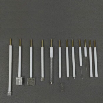
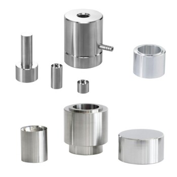
Related Products
- RF PECVD System Radio Frequency Plasma-Enhanced Chemical Vapor Deposition RF PECVD
- Chemical Vapor Deposition CVD Equipment System Chamber Slide PECVD Tube Furnace with Liquid Gasifier PECVD Machine
- Microwave Plasma Chemical Vapor Deposition MPCVD Machine System Reactor for Lab and Diamond Growth
- Cylindrical Resonator MPCVD Machine System Reactor for Microwave Plasma Chemical Vapor Deposition and Lab Diamond Growth
- Aluminized Ceramic Evaporation Boat for Thin Film Deposition
People Also Ask
- What are the benefits of PECVD? Achieve Superior Low-Temperature Thin Film Deposition
- How does RF power create plasma? Achieve Stable, High-Density Plasma for Your Applications
- Why does PECVD commonly use RF power input? For Precise Low-Temperature Thin Film Deposition
- Why is PECVD environment friendly? Understanding the Eco-Friendly Benefits of Plasma-Enhanced Coating
- What is an example of PECVD? RF-PECVD for High-Quality Thin Film Deposition