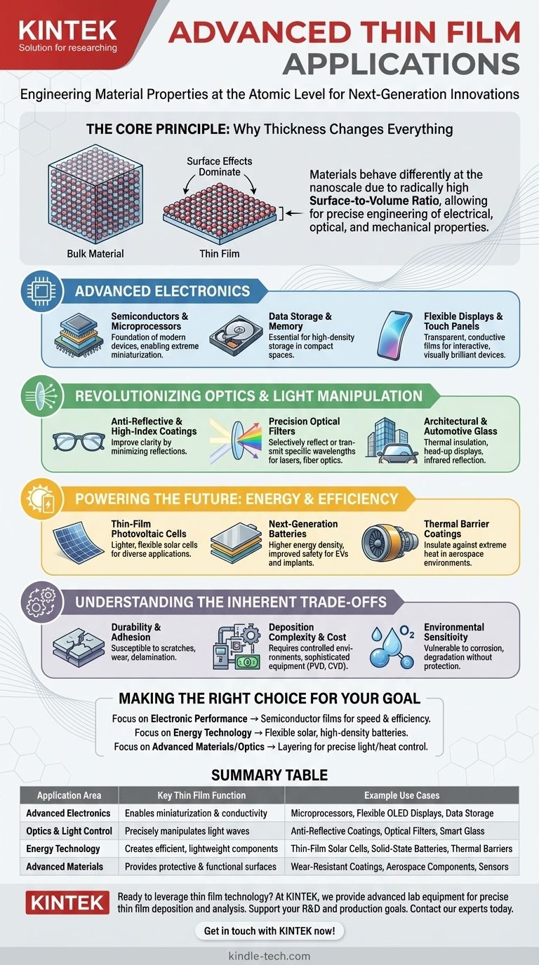
At their core, advanced thin film applications are about engineering material properties at the atomic level. While used in familiar items like mirrors and eyeglasses, their true power is in enabling next-generation electronics, high-efficiency solar cells, advanced sensors, and protective coatings for extreme environments. These applications are possible because reducing a material to a film just a few atoms thick fundamentally changes how it behaves, allowing us to control its electrical, optical, and mechanical characteristics with incredible precision.
The crucial insight is that a thin film isn't just a smaller version of a bulk material; it's an entirely new material with unique, engineered properties. The ability to precisely control these properties by controlling a film's thickness is the key that unlocks its most advanced and transformative applications.
The Core Principle: Why Thickness Changes Everything
The revolutionary applications of thin films all stem from a single, fundamental concept: materials behave differently at the nanoscale. Understanding this principle is key to seeing why they are so versatile.
The Surface-to-Volume Ratio
In a bulk material, most atoms are on the inside, shielded by their neighbors. In a thin film, a massive proportion of atoms are on the surface.
This radically high surface-to-volume ratio means that surface effects, which are negligible in bulk materials, begin to dominate the film's overall behavior.
Engineering Properties at the Nanoscale
This dominance of surface atoms allows engineers and scientists to "tune" a material's properties. By precisely controlling the thickness and structure of the film, one can manipulate how it interacts with light, conducts electricity, or resists heat.
This isn't just coating a surface; it's designing a material from the atoms up to perform a specific function.
Applications in Advanced Electronics
Thin films are the bedrock of modern microelectronics. Their ability to be deposited in hyper-thin, uniform layers allows for the creation of incredibly complex and miniaturized components.
Semiconductors and Microprocessors
The transistors that power every computer, phone, and server are built from layers of semiconductor thin films. Their thinness is what allows for the extreme miniaturization that drives Moore's Law, leading to faster and more efficient devices.
Data Storage and Memory
Magnetic thin films are essential for high-density hard drives and other forms of computer memory. The specific properties of these films allow for the storage of vast amounts of data in a very small physical space.
Flexible Displays and Touch Panels
Technologies like OLED displays and the capacitive touch panels on our phones rely on transparent, conductive thin films. These films are engineered to be both optically clear and electrically responsive, enabling devices that are both interactive and visually brilliant.
Revolutionizing Optics and Light Manipulation
By depositing multiple layers of thin films, each with a specific thickness and refractive index, we can control the flow of light with extraordinary precision.
Anti-Reflective and High-Index Coatings
A common application is the anti-reflective coating on eyeglasses or camera lenses. Multiple thin film layers are designed to cause destructive interference for reflected light, allowing more light to pass through and improving clarity.
Precision Optical Filters
In scientific and telecommunications equipment, thin films are used to create distributed Bragg reflectors and narrow-bandpass filters. These devices can selectively reflect or transmit very specific wavelengths of light, a critical function for lasers and fiber optics.
Architectural and Automotive Glass
Thin films applied to architectural glass can reflect infrared radiation, providing thermal insulation that keeps buildings cooler in the summer and warmer in the winter. In cars, this technology is used for head-up displays, where information is projected onto a specially coated windshield.
Powering the Future: Energy and Efficiency
Thin films are at the forefront of developing next-generation energy solutions that are more efficient, lightweight, and versatile than traditional technologies.
Thin-Film Photovoltaic Cells
Thin-film solar cells use layers of photovoltaic material that are thousands of times thinner than traditional silicon wafers. This makes them lighter, flexible, and suitable for a wider range of applications, from portable chargers to building-integrated solar panels.
Next-Generation Batteries
Researchers are developing thin-film solid-state batteries that promise higher energy density and improved safety compared to conventional lithium-ion batteries. These could power everything from medical implants to electric vehicles.
Thermal Barrier Coatings
In high-performance environments like jet engines and aerospace components, ceramic thin films act as thermal barriers. They insulate the underlying metal alloys from extreme heat, dramatically increasing the durability and efficiency of the engines.
Understanding the Inherent Trade-offs
While powerful, thin film technology is not without its challenges. Objectively understanding these limitations is crucial for successful implementation.
Durability and Adhesion
Because they are so thin, these films can be susceptible to scratches, wear, and delamination (peeling) if the substrate is not properly prepared or if the deposition process is flawed.
Deposition Complexity and Cost
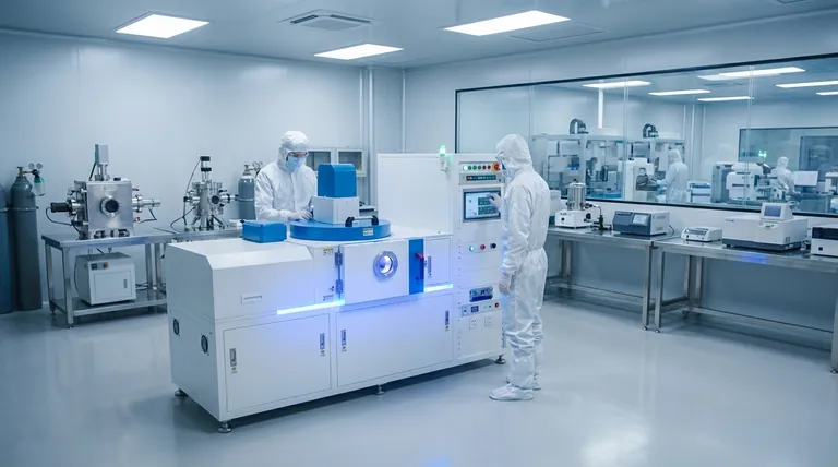
Creating high-quality, uniform thin films requires highly controlled environments and sophisticated equipment. Processes like physical vapor deposition (PVD) or chemical vapor deposition (CVD) can be complex and expensive, particularly at large scales.
Environmental Sensitivity
The high surface-to-volume ratio that grants thin films their unique properties also makes them more vulnerable to corrosion or degradation from environmental factors like moisture and oxygen if not properly protected.
Making the Right Choice for Your Goal
The application of thin films depends entirely on which of their engineered properties you need to leverage.
- If your primary focus is electronic performance: The key is using semiconductor thin films to build smaller, faster, and more power-efficient components.
- If your primary focus is energy technology: The goal is to use thin films to create lighter, more flexible solar cells and batteries with higher energy density.
- If your primary focus is advanced materials or optics: The strategy is to layer different thin films to precisely control a material's interaction with light, heat, or its physical environment.
Ultimately, thin films represent a fundamental shift from using materials as they are to designing them for exactly what we need them to do.
Summary Table:
| Application Area | Key Thin Film Function | Example Use Cases |
|---|---|---|
| Advanced Electronics | Enables miniaturization & conductivity | Microprocessors, Flexible OLED Displays, Data Storage |
| Optics & Light Control | Precisely manipulates light waves | Anti-Reflective Coatings, Optical Filters, Smart Glass |
| Energy Technology | Creates efficient, lightweight components | Thin-Film Solar Cells, Solid-State Batteries, Thermal Barriers |
| Advanced Materials | Provides protective & functional surfaces | Wear-Resistant Coatings, Aerospace Components, Sensors |
Ready to leverage thin film technology in your lab?
Thin films are the foundation of modern innovation, from flexible electronics to high-efficiency energy systems. At KINTEK, we specialize in providing the advanced lab equipment and consumables needed for precise thin film deposition and analysis. Whether you are developing next-generation semiconductors, optical coatings, or energy storage solutions, our expertise and reliable products are designed to support your most ambitious R&D and production goals.
Contact our experts today to discuss how we can help you achieve unparalleled precision and performance in your thin film applications.
Visual Guide
Related Products
- Aluminum-Plastic Flexible Packaging Film for Lithium Battery Packaging
- Thin-Layer Spectral Electrolysis Electrochemical Cell
People Also Ask
- What are the properties of Aluminium (Al) relevant to its use in coatings? High Reflectivity & Conductivity Explored
- What is organic thin film? A Guide to Engineered Molecular Layers for Advanced Tech
- What is the thinnest coating? Unlocking Unique Properties at the Atomic Scale
- What are the three types of lamination? Choose the Perfect Finish for Your Print Project
- Is there a way to test lithium batteries? Understand Voltage vs. True Health

