At its core, Low-Pressure Chemical Vapor Deposition (LPCVD) excels due to its ability to produce exceptionally high-quality and uniform thin films at a large scale. This method is renowned for its cost-effectiveness, versatility, and ability to coat complex surfaces, making it a foundational process in the semiconductor and solar industries. The primary advantages stem directly from the low-pressure environment in which it operates.
The defining advantage of LPCVD is not a single feature, but how its low-pressure environment fundamentally improves gas transport. This change enables the deposition of highly uniform, pure, and conformal films, making it an indispensable tool for modern microfabrication.
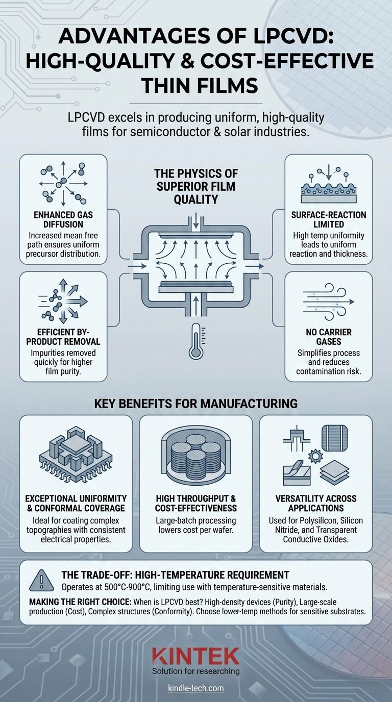
The Physics Behind LPCVD's Superior Film Quality
To understand why LPCVD is so effective, we must look at how the low-pressure environment alters the behavior of the reactant gases inside the deposition chamber.
Enhanced Gas Diffusion
Operating at low pressure significantly increases the mean free path of gas molecules, which is the average distance a molecule travels before colliding with another.
This allows precursor gases to diffuse more freely and quickly throughout the reaction chamber, reaching every surface of the substrates with much greater uniformity than at atmospheric pressure.
Surface-Reaction Limited Growth
LPCVD processes are typically run at high temperatures where the deposition rate is limited by the chemical reaction rate on the substrate surface, not by the rate of gas transport to the surface.
Because the temperature is highly uniform across the substrates, the surface reaction proceeds at the same rate everywhere. This is the fundamental reason LPCVD achieves excellent film thickness uniformity across a wafer and from wafer to wafer.
Efficient By-product Removal
The improved gas diffusion at low pressure also means that reaction by-products and impurities are removed from the reaction zone much more rapidly.
This results in higher purity films, a critical requirement for high-performance electronic devices.
Elimination of Carrier Gases
Unlike many other CVD methods, LPCVD typically does not require an inert carrier gas (like nitrogen or argon) to transport the reactants.
Eliminating the carrier gas simplifies the process and, more importantly, removes a major potential source of particle contamination, further improving film quality.
Key Benefits for Manufacturing
The physical principles of LPCVD translate directly into tangible advantages for high-volume manufacturing environments.
Exceptional Uniformity and Conformal Coverage
LPCVD is unmatched in its ability to deposit films that are highly conformal, meaning the film perfectly coats the steps, trenches, and complex 3D topography of a modern microchip.
This is a direct result of the surface-reaction limited kinetics. The process also delivers outstanding uniformity in film thickness and electrical properties (like resistivity) across very large batches of wafers.
High Throughput and Cost-Effectiveness
LPCVD systems typically use horizontal or vertical tube furnaces that can process large batches of wafers—often 100 to 200 at a time—stacked closely together.
This ability to process wafers in large, dense batches leads to very high throughput and a significantly lower cost per wafer, making it an economically favorable choice for mass production.
Versatility Across Applications
The process is highly versatile, used for depositing a wide range of materials critical for manufacturing.
Common applications include polysilicon for transistor gates, silicon nitride for insulation and passivation layers, and transparent conductive oxides for solar cells. Its ability to create these high-quality films makes it a preferred choice across many industries.
Understanding the Trade-offs
No process is perfect. To use LPCVD effectively, it is critical to understand its primary limitation.
The High-Temperature Requirement
The most significant disadvantage of LPCVD is its reliance on high process temperatures, often in the range of 500°C to 900°C.
This high thermal budget restricts its use to substrates and devices that can withstand such heat. It cannot be used for depositions on temperature-sensitive materials like polymers or on fully fabricated devices that contain low-melting-point metals like aluminum.
Making the Right Choice for Your Goal
Selecting the right deposition method depends entirely on the specific requirements of your film and substrate.
- If your primary focus is fabricating high-density semiconductor devices: LPCVD is often the superior choice due to its exceptional purity and ability to conformally coat complex 3D structures.
- If your primary focus is large-scale production where cost per unit is critical: LPCVD's high-throughput batch processing makes it an extremely cost-effective solution for applications like solar cells and memory devices.
- If your primary focus is depositing films on temperature-sensitive substrates: You must explore lower-temperature alternatives like Plasma-Enhanced CVD (PECVD), as the high heat of LPCVD is a non-negotiable constraint.
By understanding these principles, you can confidently leverage LPCVD for its unique combination of quality, scale, and cost-efficiency.
Summary Table:
| Advantage | Key Benefit | Ideal For |
|---|---|---|
| Enhanced Gas Diffusion | Superior film thickness uniformity | High-density semiconductor devices |
| Surface-Reaction Limited Growth | Conformal coverage on complex 3D structures | Microchip fabrication with intricate topography |
| High-Throughput Batch Processing | Lower cost per wafer for mass production | Solar cells and memory device manufacturing |
| Efficient By-product Removal | Higher purity films for electronic devices | Applications requiring minimal contamination |
Ready to enhance your microfabrication process with LPCVD technology?
KINTEK specializes in advanced lab equipment and consumables for semiconductor and solar industries. Our expertise in LPCVD systems can help you achieve:
- Exceptional film uniformity across large wafer batches
- Cost-effective production with high-throughput capabilities
- Superior conformal coatings for complex 3D structures
Let us help you optimize your deposition process for maximum quality and efficiency. Contact our experts today to discuss how our LPCVD solutions can meet your specific manufacturing needs!
Visual Guide
Related Products
- Inclined Rotary Plasma Enhanced Chemical Vapor Deposition PECVD Equipment Tube Furnace Machine
- Inclined Rotary Plasma Enhanced Chemical Vapor Deposition PECVD Equipment Tube Furnace Machine
- Chemical Vapor Deposition CVD Equipment System Chamber Slide PECVD Tube Furnace with Liquid Gasifier PECVD Machine
- Laboratory CVD Boron Doped Diamond Materials
- Microwave Plasma Chemical Vapor Deposition MPCVD Machine System Reactor for Lab and Diamond Growth
People Also Ask
- Why is a PECVD system required for vertical graphene synthesis? Master Directional Control for 3D Nanostructures
- How does plasma enhanced chemical vapor deposition work? Enable Low-Temperature Thin Film Deposition
- What is plasma enhanced chemical vapor deposition PECVD equipment? A Guide to Low-Temperature Thin Film Deposition
- What are the advantages of plasma enhanced chemical vapor deposition? Enable Low-Temperature, High-Quality Film Deposition
- What is the necessity of depositing a silicon nitride (SiNx) thin film using PECVD? Optimize QSSPC Lifetime Measurement


