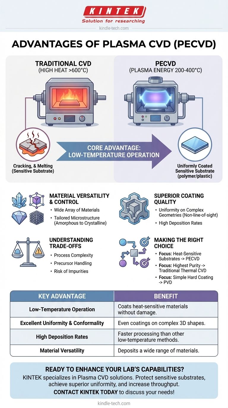
The primary advantage of Plasma-Enhanced Chemical Vapor Deposition (PECVD) is its ability to deposit high-quality, uniform thin films at significantly lower temperatures than traditional CVD methods. This makes it possible to coat materials that would otherwise be damaged by extreme heat, unlocking a vast range of applications in electronics, optics, and material science.
PECVD uses an energy-rich plasma to drive chemical reactions, bypassing the need for extreme heat. This fundamental difference makes it the ideal choice for coating temperature-sensitive materials without sacrificing the versatility and quality inherent to CVD processes.
The Core Advantage: Overcoming Temperature Limitations
How Plasma Replaces Heat
In traditional Chemical Vapor Deposition (CVD), very high temperatures (often >600°C) are required to provide the thermal energy needed for precursor gases to react and form a solid film.
PECVD creates a plasma, an ionized gas, which is a highly energetic state of matter. This plasma provides the activation energy for the reaction, allowing the deposition to occur at much lower substrate temperatures, typically in the 200-400°C range.
Protecting Temperature-Sensitive Substrates
This lower operating temperature is the single most critical advantage of PECVD. It allows for the deposition of high-quality films on materials like polymers, plastics, and fully fabricated semiconductor devices that cannot withstand the heat of conventional CVD.
Unlocking Material Versatility and Control
A Broad Palette of Materials
PECVD is an exceptionally versatile technique. It can be used to deposit a wide array of materials, including elemental solids, alloys, glassy compounds, and complex polymers.
Tailoring the Microstructure
By carefully controlling the plasma conditions and gas chemistry, operators can precisely tune the final structure of the deposited film. This allows for the creation of materials ranging from completely amorphous (glassy) to polycrystalline or even single-crystal films.
Achieving Superior Coating Quality
Uniformity on Complex Geometries
Like all CVD processes, PECVD is a non-line-of-sight technique. This means the precursor gases can flow around and into complex, three-dimensional shapes, ensuring a highly uniform and conformal coating even on intricate surfaces and in internal cavities.
High Deposition Rates
The highly reactive plasma environment often leads to significantly higher deposition rates compared to other low-temperature methods like Low-Pressure CVD (LPCVD), improving manufacturing throughput.
Understanding the Inherent Trade-offs
Process Complexity
The benefits of PECVD come at the cost of complexity. Achieving a desired film requires precise control over numerous variables, including gas composition, flow rates, pressure, RF power, and heating profiles.
Precursor and By-product Handling
The chemical precursors used in PECVD can be expensive, unstable, or hazardous. Furthermore, the process generates by-products and waste gases that require safe handling and disposal.
Risk of Impurities
If the process parameters are not perfectly optimized, the precursor gases may not decompose completely. This can lead to the incorporation of undesirable impurities, such as hydrogen, into the deposited film, which can affect its properties.
Making the Right Choice for Your Goal
When selecting a deposition method, your specific goal is the most important factor.
- If your primary focus is coating temperature-sensitive substrates: PECVD is almost always the superior choice due to its low-temperature operation.
- If your primary focus is achieving the highest possible film purity for a durable material: Traditional high-temperature thermal CVD may offer a cleaner result by avoiding plasma-induced complexities.
- If your primary focus is a simple, hard coating on a metal part: Physical Vapor Deposition (PVD) might be a more straightforward and cost-effective alternative.
Ultimately, choosing PECVD is a deliberate engineering decision to gain temperature flexibility and material control.
Summary Table:
| Key Advantage | Benefit |
|---|---|
| Low-Temperature Operation | Coats heat-sensitive materials like polymers and plastics without damage. |
| Excellent Uniformity & Conformality | Non-line-of-sight process ensures even coatings on complex 3D shapes. |
| High Deposition Rates | Faster processing than other low-temperature methods like LPCVD. |
| Material Versatility | Deposits a wide range of materials, from amorphous to crystalline films. |
Ready to enhance your lab's capabilities with low-temperature, high-quality thin films?
KINTEK specializes in providing advanced lab equipment and consumables for cutting-edge research and development. Our expertise in Plasma CVD solutions can help you:
- Protect sensitive substrates with precise, low-temperature deposition processes.
- Achieve superior coating uniformity on even the most complex geometries.
- Increase your throughput with reliable, high-performance systems.
Let our team help you select the perfect equipment to meet your specific material science goals. Contact KINTEK today to discuss your Plasma CVD needs!
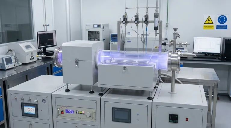
Visual Guide
Related Products
- Microwave Plasma Chemical Vapor Deposition MPCVD Machine System Reactor for Lab and Diamond Growth
- 915MHz MPCVD Diamond Machine Microwave Plasma Chemical Vapor Deposition System Reactor
- Chemical Vapor Deposition CVD Equipment System Chamber Slide PECVD Tube Furnace with Liquid Gasifier PECVD Machine
- Cylindrical Resonator MPCVD Machine System Reactor for Microwave Plasma Chemical Vapor Deposition and Lab Diamond Growth
- RF PECVD System Radio Frequency Plasma-Enhanced Chemical Vapor Deposition RF PECVD
People Also Ask
- Why is argon-rich gas phase chemistry used for UNCD growth? Unlock Precision Nano-Diamond Synthesis
- How are CVD diamonds created? Discover the Science of Lab-Grown Diamond Precision
- How is a diamond formed from CVD? The Science of Growing Diamonds Atom by Atom
- What are the advantages of a Microwave Plasma CVD reactor for MCD/NCD coatings? Precision Multilayer Diamond Engineering
- What pressure is needed for chemical vapor deposition of diamonds? Master the Low-Pressure 'Sweet Spot'


