The primary advantage of using an electrolytic polishing device for EK-181 steel is the elimination of mechanical deformation during sample preparation. By thinning the sample through electrochemical reactions in a solution of chromic anhydride and phosphoric acid, this method avoids the structural damage inherent to mechanical polishing, ensuring the final Transmission Electron Microscopy (TEM) images reflect the material's true state.
Core Takeaway Mechanical thinning introduces artificial defects that can skew analysis, but electrolytic polishing thins EK-181 steel without physical stress. This non-destructive approach is essential for preserving the original dislocation density and successfully imaging fine, 5–10 nm MX-type precipitates.
Preserving Microstructural Integrity
Avoiding Induced Deformation
The most significant risk in preparing TEM samples is altering the material while trying to measure it. Mechanical polishing involves abrasion, which physically forces material away.
This mechanical force inevitably introduces additional deformation damage to the specimen. Electrolytic polishing bypasses this entirely by removing material chemically, leaving the internal structure undisturbed.
Maintaining True Dislocation Density
For metallurgists, accurate dislocation density is a critical metric for understanding material strength and behavior.
Because electrolytic polishing does not apply physical stress, it preserves the original dislocation density of the EK-181 steel. This ensures that the dislocation networks observed under the microscope are inherent to the steel, not artifacts created during the preparation process.
Enhancing High-Resolution Observation
Revealing Nanometer-Sized Precipitates
EK-181 steel contains extremely small structural features that are easily obscured by poor preparation.
Electrolytic polishing preserves the state of nanometer-sized precipitates. This clarity is vital for analyzing the material's hardening mechanisms and thermal stability.
Visualizing MX-Type Particles
The precision of this method allows for the clear observation of specific 5–10 nm MX-type particles.
Achieving this level of resolution requires a pristine surface free from the "smeared" layers often left behind by mechanical methods. Electrolytic polishing provides the clean, thin foil necessary for the electron beam to resolve these minute features.
Understanding the Trade-offs
Chemical Handling Requirements
While superior for structural preservation, this method utilizes a specific electrolyte solution of chromic anhydride and phosphoric acid.
These are potent chemicals that require careful handling and safety protocols. Unlike mechanical polishing, which creates physical dust, this process involves managing hazardous liquid waste and ensuring proper ventilation during the electrochemical reaction.
Making the Right Choice for Your Goal
To maximize the quality of your TEM analysis on EK-181 steel, align your preparation method with your specific analytical targets:
- If your primary focus is measuring dislocation density: Choose electrolytic polishing to ensure the defects you count are real and not introduced by grinding or polishing stress.
- If your primary focus is precipitate analysis: Rely on this method to clearly resolve 5–10 nm MX-type particles without surface artifacts obscuring them.
- If your primary focus is avoiding artifacts: Use this technique to eliminate the risk of deformation damage common in mechanical thinning.
By removing mechanical stress from the equation, electrolytic polishing transforms sample preparation from a destructive process into a method of true structural revelation.
Summary Table:
| Feature | Electrolytic Polishing | Mechanical Polishing |
|---|---|---|
| Material Removal | Electrochemical reaction (CrO3 + H3PO4) | Physical abrasion |
| Structural Damage | Zero mechanical deformation | Potential induced deformation |
| Dislocation Integrity | Preserves original density | Skewed by physical stress |
| Precipitate Clarity | High (5-10 nm MX-type visible) | Lower (surface artifacts) |
| Ideal Application | High-resolution microstructural analysis | Bulk material removal |
Elevate Your Microstructural Analysis with KINTEK
Precision in TEM imaging begins with flawless sample preparation. At KINTEK, we specialize in high-performance laboratory solutions designed for the most demanding materials research. Whether you are analyzing 5–10 nm MX-type precipitates or measuring dislocation density in EK-181 steel, our advanced electrolytic cells and electrodes provide the electrochemical precision you need to eliminate mechanical artifacts.
From high-temperature furnaces for alloy development to specialized crushing and milling systems and PTFE consumables, KINTEK is your partner in achieving true structural revelation.
Ready to enhance your lab's efficiency and data accuracy? Contact our experts today to find the perfect equipment for your research goals.
References
- Н. А. Полехина, K. A. Moroz. The Microstructure, Tensile and Impact Properties of Low-Activation Ferritic-Martensitic Steel EK-181 after High-Temperature Thermomechanical Treatment. DOI: 10.3390/met12111928
This article is also based on technical information from Kintek Solution Knowledge Base .
Related Products
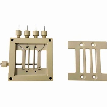
- Electrode Polishing Material for Electrochemical Experiments
- Laboratory Grinding Mill Mortar Grinder for Sample Preparation
- Sample Support Body for Electrochemical Tests
- Cylindrical Lab Electric Heating Press Mold for Laboratory Applications
- Quartz Electrolytic Electrochemical Cell for Electrochemical Experiments
People Also Ask
- What is the purpose of using electrolytic polishing on copper foils? Optimize Your CVD Graphene & hBN Growth Surface
- What criteria are used during the visual inspection of electrodes? Essential Quality Assessment for Your Lab
- How do you prepare the polishing setup for an electrode? Achieve a Flawless Mirror Finish for Reliable Electrochemistry
- Which types of materials are basically polished by electrolytic polishing? A Guide to Metals & Alloys
- What are the examples of electrode materials? From Platinum to Graphite for Your Application