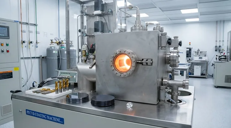
At its core, Chemical Vapor Deposition (CVD) is a cornerstone technology used to create exceptionally pure, high-performance thin films and coatings. Its applications are widespread, serving as a critical process in industries ranging from semiconductor manufacturing, where it's used to build microchips layer by layer, to the production of advanced materials like high-quality lab-grown diamonds.
CVD's value is not just in what it creates, but how it creates it. Its true strength lies in its unmatched control, allowing for the cost-effective and scalable production of highly pure, uniform coatings on virtually any surface, from a flat wafer to a complex 3D object.
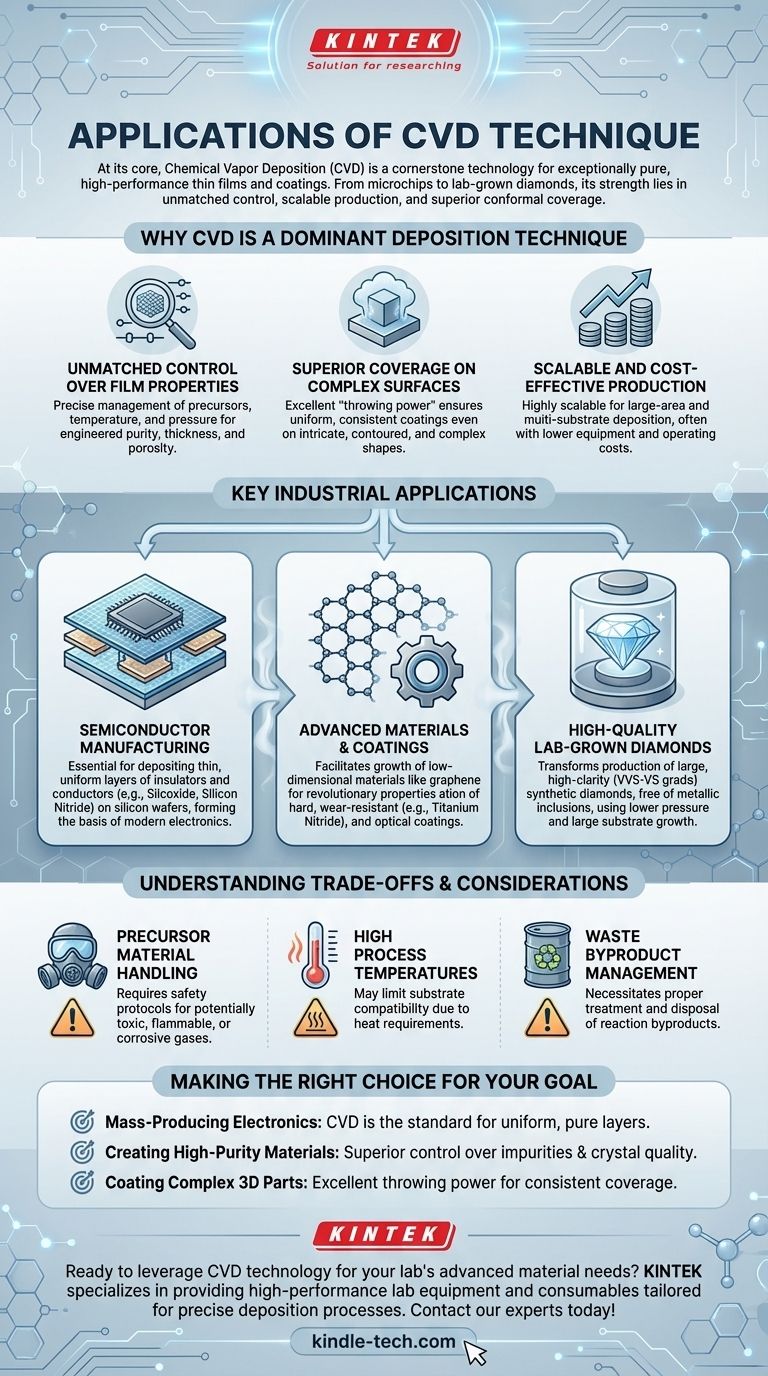
Why CVD is a Dominant Deposition Technique
The versatility of CVD stems from a few fundamental advantages that make it the ideal choice for a wide range of high-tech applications. These core characteristics explain its widespread adoption.
Unmatched Control Over Film Properties
CVD allows for meticulous control over the final product. By precisely managing precursor gases, temperature, and pressure, manufacturers can dictate the film's purity, thickness, and even porosity.
This means you can engineer materials with highly specific and versatile properties, tailored exactly to the needs of the application.
Superior Coverage on Complex Surfaces
The technique is characterized by its excellent "throwing power." This term describes its ability to deposit a perfectly uniform film over all surfaces of a substrate, even those with complex, contoured, or intricate shapes.
Unlike line-of-sight deposition methods, the chemical vapor precursor envelops the object, ensuring a consistent coating with low porosity everywhere. This is critical for protecting parts from corrosion or wear.
Scalable and Cost-Effective Production
CVD is built for industrial production. It is highly scalable, allowing for deposition over large areas and on multiple substrates at once, leading to high production efficiency.
Compared to other high-performance methods like High-Pressure/High-Temperature (HPHT) for diamond synthesis, CVD often involves lower equipment costs and operates at much lower pressures, making it a more accessible and cost-effective choice for many processes.
Key Industrial Applications
These fundamental strengths enable CVD to be a go-to solution in several critical industries.
Semiconductor Manufacturing
This is the quintessential application of CVD. The entire microelectronics industry relies on CVD to deposit thin films of materials like silicon dioxide and silicon nitride onto silicon wafers.
These layers act as insulators, conductors, and barriers that form the microscopic structures of transistors and integrated circuits. The purity and uniformity provided by CVD are non-negotiable for modern electronics.
Advanced Materials and Coatings
CVD is a key enabler for creating next-generation materials. It is widely used for the efficient growth of low-dimensional materials, such as graphene, which have revolutionary electronic and mechanical properties.
Furthermore, it is used to apply hard, wear-resistant coatings (like titanium nitride) to cutting tools, or to create optical coatings with specific reflective or anti-reflective properties.
High-Quality Lab-Grown Diamonds
CVD has transformed the production of synthetic diamonds. The process allows for the growth of large, high-clarity (VVS-VS grade) diamonds that are free of the metallic inclusions often found in diamonds made with other methods.
Because it operates at low pressure (under 27 kPa), it provides precise control over chemical impurities and allows for growth over large, flat substrates, making it an efficient production method.
Understanding the Trade-offs and Considerations
While powerful, CVD is not a universal solution. A clear-eyed technical assessment requires understanding its operational demands.
Precursor Material Handling
The "vapor" in CVD comes from precursor chemicals that are often toxic, flammable, or corrosive gases. This necessitates significant investment in safety protocols, gas handling systems, and abatement infrastructure, which can add complexity and cost.
High Process Temperatures
Although it's a low-pressure method, most CVD processes still require high temperatures to drive the necessary chemical reactions. This can limit the types of substrate materials that can be coated, as some may not withstand the heat without deforming or melting.
Waste Byproduct Management
The chemical reactions that deposit the film also create byproducts. These waste streams must be properly managed, treated, and disposed of, which is an important environmental and regulatory consideration for any industrial CVD operation.
Making the Right Choice for Your Goal
Selecting a deposition technique depends entirely on your end goal. CVD excels where precision, purity, and conformal coverage are paramount.
- If your primary focus is mass-producing electronics: CVD is the industry standard for depositing the uniform, pure insulating and conductive layers essential for semiconductor wafers.
- If your primary focus is creating high-purity materials like lab-grown diamonds or graphene: CVD offers superior control over chemical impurities and crystal quality at lower pressures than alternative methods.
- If your primary focus is coating complex, three-dimensional parts: CVD's excellent throwing power ensures a consistent, high-quality film even on intricate or contoured surfaces where other methods fail.
Ultimately, CVD's power lies in its ability to translate precise chemical control into tangible, high-value physical materials at an industrial scale.
Summary Table:
| Application Area | Key Use Case | CVD Advantage |
|---|---|---|
| Semiconductor Manufacturing | Depositing insulating & conductive layers on wafers | Unmatched purity and uniformity |
| Advanced Materials & Coatings | Creating graphene, hard coatings (e.g., titanium nitride) | Precise control over film properties |
| Lab-Grown Diamonds | Producing high-clarity, VVS-VS grade diamonds | Lower pressure operation, superior crystal quality |
| Complex 3D Part Coatings | Uniform coverage on intricate surfaces | Excellent conformal coverage ('throwing power') |
Ready to leverage CVD technology for your lab's advanced material needs? KINTEK specializes in providing high-performance lab equipment and consumables tailored for precise deposition processes. Whether you're developing next-generation semiconductors, advanced coatings, or high-purity materials, our solutions ensure scalability, cost-efficiency, and superior results. Contact our experts today to discuss how we can support your specific application requirements!
Visual Guide
Related Products
- Chemical Vapor Deposition CVD Equipment System Chamber Slide PECVD Tube Furnace with Liquid Gasifier PECVD Machine
- Customer Made Versatile CVD Tube Furnace Chemical Vapor Deposition Chamber System Equipment
- Microwave Plasma Chemical Vapor Deposition MPCVD Machine System Reactor for Lab and Diamond Growth
- 915MHz MPCVD Diamond Machine Microwave Plasma Chemical Vapor Deposition System Reactor
- Custom CVD Diamond Coating for Lab Applications
People Also Ask
- Why is Chemical Vapor Deposition (CVD) equipment uniquely suited for constructing hierarchical superhydrophobic structures?
- What happens during deposition chemistry? Building Thin Films from Gaseous Precursors
- What is the chemical vapor deposition growth process? Build Superior Thin Films from the Atom Up
- What types of substrates are used in CVD to facilitate graphene films? Optimize Graphene Growth with the Right Catalyst
- How are carbon nanotubes grown? Master Scalable Production with Chemical Vapor Deposition


