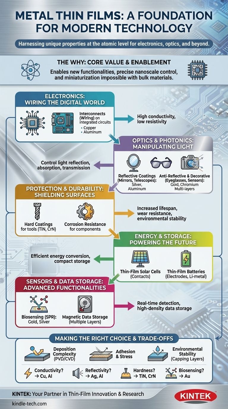
In short, metal thin films are a cornerstone of modern technology. Their applications span from the microchips in your phone and the anti-reflective coating on your glasses to the protective layers on industrial tools and the reflective surfaces of mirrors. By depositing a metal layer just atoms or micrometers thick onto a substrate, we can harness the unique electrical, optical, and mechanical properties of that metal in a highly controlled and efficient manner.
The core value of metal thin films is not just in saving material, but in enabling entirely new functionalities. By controlling a metal's structure at the nanoscale, we can precisely engineer its interaction with light, electricity, and its environment, creating components that are impossible to make with bulk materials.
The Foundation: Why Use a Film Instead of Bulk Metal?
The decision to use a thin film is driven by the need to impart a metal's properties onto the surface of another material, known as a substrate. This approach offers benefits that bulk metal cannot.
Harnessing Desired Properties
The primary goal is to leverage a metal's inherent characteristics. For instance, a thin film of aluminum or silver is used to make a glass surface highly reflective for a mirror. A thin film of copper is used to create conductive pathways on a silicon wafer for an integrated circuit.
Efficiency and Miniaturization
Using a film that is nanometers to micrometers thick uses drastically less material than a solid block, reducing cost and weight. More importantly, this thinness is what enables the miniaturization of modern electronics, allowing billions of transistors and their connections to fit on a single chip.
Engineering New Behaviors
At very small thicknesses, the properties of a film can differ from its bulk counterpart. The way light or electrons behave can be manipulated by precisely controlling the film's thickness and structure, leading to unique optical filters or advanced sensors.
Key Application Domains Explained
The versatility of metal thin films means they are found across numerous high-tech industries. Understanding the function in each domain reveals the depth of their impact.
Electronics: The Wiring of the Digital World
This is arguably the most significant application. Thin metal films act as the interconnects, or wiring, that link transistors and other components on an integrated circuit.
Metals like copper and aluminum are chosen for their high electrical conductivity and their compatibility with semiconductor manufacturing processes. Without this technology, modern microprocessors, memory chips, and displays would not exist.
Optics and Photonics: Manipulating Light
Metal films are fundamental to controlling light. Their applications are based on their ability to reflect, absorb, or transmit light in specific ways.
- Reflective Coatings: A thin, uniform layer of aluminum or silver on glass creates a high-quality mirror for household use, telescopes, and automotive headlamps.
- Anti-Reflective Coatings: While often using metal oxides, these multi-layer systems can incorporate ultra-thin metal layers to reduce glare on eyeglasses, camera lenses, and solar panels.
- Decorative & Architectural Coatings: Thin films of metals like chromium, titanium, or even gold provide durable, colored, or reflective finishes on everything from jewelry and bathroom fixtures to energy-efficient architectural glass that reflects thermal radiation.
Protection and Durability: Shielding Surfaces
Many applications require a surface that is harder, more durable, or more resistant to environmental degradation than the underlying material.
Metal and metal-compound films (like nitrides) create hard coatings on cutting tools and industrial drills, dramatically increasing their lifespan and performance. Similarly, they serve as protective films to prevent corrosion on machine parts and electronic components.
Energy and Storage: Powering the Future
Metal thin films are critical components in renewable energy and energy storage.
- Thin-Film Solar Cells: They serve as the electrical contacts that collect the current generated when light hits the semiconductor material. Transparent conductive oxides (a related class of thin film) act as the top electrode, allowing light to pass through.
- Thin-Film Batteries: In next-generation solid-state batteries, thin films of lithium metal or other compounds act as the electrodes, enabling smaller, lighter, and potentially safer energy storage.
Advanced Sensors and Data Storage
The unique properties of thin films also enable advanced applications.
- Magnetic Storage: Hard drives use multiple layers of magnetic thin films to store data as magnetic domains.
- Biosensors: Thin films of gold or silver are used in a technique called surface plasmon resonance (SPR), which can detect the binding of biological molecules in real time for medical diagnostics and research.
Understanding the Trade-offs
While powerful, thin film technology is not without its challenges. The process of creating a high-quality film is a precise science.
Deposition Complexity
Creating a uniform, pure, and defect-free film requires sophisticated equipment and highly controlled environments. Techniques like Physical Vapor Deposition (PVD) or Chemical Vapor Deposition (CVD) occur in a vacuum and are complex, capital-intensive processes.
Adhesion and Stress
The film must adhere perfectly to the substrate without peeling or cracking. Differences in thermal expansion between the film and the substrate can create internal stress, leading to mechanical failure over the device's lifetime.
Environmental Stability
A very thin layer of metal has an enormous surface-area-to-volume ratio, making it more susceptible to oxidation and corrosion than a bulk material. For many applications, protective "capping layers" are required to ensure long-term stability.
Making the Right Choice for Your Goal
The specific metal and deposition method are chosen based on the desired outcome. Your primary goal will dictate the optimal approach.
- If your primary focus is high conductivity for electronics: Copper and aluminum are the industry standards for interconnects in microchips due to their low resistivity and mature manufacturing processes.
- If your primary focus is manipulating light: Silver and aluminum provide the highest reflectivity for mirrors, while multi-layer stacks of dielectrics and ultra-thin metals are needed for advanced filters and anti-reflection coatings.
- If your primary focus is surface hardness and wear resistance: Titanium nitride (TiN) and chromium nitride (CrN) are leading choices for hard coatings on tools and mechanical components.
- If your primary focus is biosensing or plasmonics: Gold is the preferred material due to its chemical inertness and excellent plasmonic properties, ensuring stable and reliable sensor performance.
Ultimately, metal thin films are a foundational enabling technology, allowing us to build the modern world one atomic layer at a time.
Summary Table:
| Application Domain | Key Functions | Common Metals Used |
|---|---|---|
| Electronics | Interconnects & wiring on microchips | Copper, Aluminum |
| Optics & Photonics | Reflective/anti-reflective coatings, decorative finishes | Silver, Aluminum, Gold, Chromium |
| Protection & Durability | Hard coatings for tools, corrosion resistance | Titanium Nitride (TiN), Chromium Nitride (CrN) |
| Energy & Storage | Electrodes for solar cells & batteries | Various (e.g., for contacts in thin-film solar cells) |
| Sensors & Data Storage | Biosensing (SPR), magnetic data storage | Gold, Silver |
Ready to Engineer Your Next Innovation with Metal Thin Films?
Whether you are developing advanced microelectronics, high-performance optical coatings, durable protective layers, or cutting-edge sensors, the precise application of metal thin films is critical to your success. KINTEK specializes in providing high-quality lab equipment and consumables for thin-film deposition and research, serving the precise needs of laboratories and R&D teams.
We can help you select the right materials and processes to achieve superior conductivity, reflectivity, hardness, or sensing capabilities for your specific project. Let our expertise support your development from concept to reality.
Contact KINTEK today to discuss your requirements and discover how our solutions can enhance your research and production outcomes.
Visual Guide
Related Products
- Molybdenum Tungsten Tantalum Evaporation Boat for High Temperature Applications
- Tungsten Evaporation Boat for Thin Film Deposition
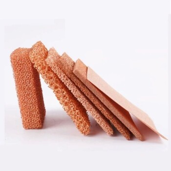
- Copper Foam
- Electron Beam Evaporation Coating Oxygen-Free Copper Crucible and Evaporation Boat
- Copper Nickel Foam Metal Sheet
People Also Ask
- How source material is evaporated during deposition? A Guide to Resistive vs. E-Beam Methods
- Is thermal evaporation used to deposit a thin metal film? A Guide to This Foundational PVD Technique
- What is the widely used boat made of in thermal evaporation? Choosing the Right Material for High-Purity Deposition
- What are thermal evaporation sources? Key Types and How to Choose the Right One
- What is the difference between thermal evaporation and e beam evaporation? Choose the Right Method for Your Thin Film