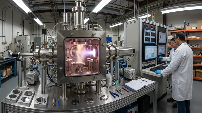
At its core, Physical Vapor Deposition (PVD) is a family of vacuum-based coating processes. The primary types are distinguished by how they generate the material vapor: either by "boiling" a source material (evaporation) or by "blasting" it with ions (sputtering). The most common industrial techniques include Cathodic Arc Evaporation, Electron Beam Evaporation, and Magnetron Sputtering.
The essential difference between PVD techniques lies in the method used to transform solid material into a vapor. This choice directly controls the energy of the depositing particles, which in turn determines critical film properties like density, adhesion, and uniformity.
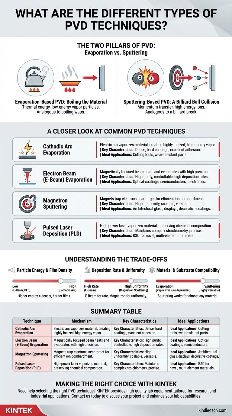
The Two Pillars of PVD: Evaporation vs. Sputtering
Understanding the various PVD methods begins with grasping the two fundamental mechanisms for creating a vapor from a solid source material inside a vacuum chamber.
Evaporation-Based PVD: Boiling the Material
In evaporation processes, the source material (known as the target or evaporant) is heated until its atoms boil off and travel through the vacuum to coat the substrate.
The energy applied is thermal, resulting in relatively low-energy vapor particles. The process is analogous to water boiling into steam in a kettle.
Sputtering-Based PVD: A Billiard Ball Collision
Sputtering involves a momentum transfer process. High-energy ions, typically from an inert gas like Argon, are accelerated to bombard the source material.
This bombardment is like a high-speed billiard ball break, physically knocking atoms off the target. These "sputtered" atoms then travel and deposit onto the substrate.
A Closer Look at Common PVD Techniques
While all PVD methods fall under the umbrella of evaporation or sputtering, specific technologies have been developed to control the process for different applications.
Cathodic Arc Evaporation
This is an evaporation technique that uses a high-current, low-voltage electric arc to vaporize the source material.
The process creates a highly ionized vapor, meaning the depositing particles have a high kinetic energy. This results in extremely dense and hard coatings with excellent adhesion, ideal for cutting tools and wear-resistant components.
Electron Beam (E-Beam) Evaporation
E-Beam PVD uses a magnetically focused beam of electrons to heat and evaporate the source material with high precision.
It is a clean, controllable process capable of achieving very high deposition rates. This makes it a preferred method for high-purity optical coatings, semiconductors, and other electronic applications.
Magnetron Sputtering
This is the most widely used sputtering technique. It uses powerful magnets behind the target to trap electrons in a plasma field near the target's surface.
This magnetic confinement dramatically increases the efficiency of the ion bombardment process, allowing for faster deposition rates and better coverage over large, complex surfaces. It is a versatile workhorse for everything from decorative coatings to architectural glass.
Pulsed Laser Deposition (PLD)
Sometimes called laser ablation, this method uses a high-power laser focused on the target to vaporize material.
PLD is exceptionally good at preserving the chemical composition (stoichiometry) of complex, multi-element materials. While not as common for large-scale industrial production, it is a vital tool in research and development for novel materials.
Understanding the Trade-offs
Choosing a PVD method is a matter of balancing competing factors. No single technique is universally superior; the best choice is dictated by the desired outcome.
Particle Energy and Film Density
Techniques that produce highly ionized vapor, like Cathodic Arc Evaporation, result in higher-energy particles. This energy helps create denser, more adherent, and harder films.
Evaporation methods like E-Beam PVD produce lower-energy vapor, which is less damaging to sensitive substrates but may result in less dense films without additional energy input (like ion assistance).
Deposition Rate and Uniformity
Magnetron Sputtering is well-known for its ability to produce highly uniform coatings over large areas, making it ideal for industries like architectural glass or displays.
E-Beam Evaporation can achieve very high deposition rates, but controlling uniformity can be more challenging. Cathodic Arc often produces "macro-particles" (small droplets) that can affect surface finish, requiring post-processing for some applications.
Material and Substrate Compatibility
Sputtering is highly versatile and can be used to deposit almost any material, including alloys and compounds.
Evaporation works best for materials with suitable vapor pressures and can be challenging for complex alloys where elements evaporate at different rates.
Making the Right Choice for Your Application
The selection of a PVD technique is driven entirely by the required properties of the final coating.
- If your primary focus is maximum hardness and wear resistance: Cathodic Arc Evaporation is often the best choice due to the high-energy, ionized vapor it produces.
- If your primary focus is high-purity optical or electronic films: Electron Beam (E-Beam) PVD offers the control and cleanliness required for these demanding applications.
- If your primary focus is uniform coating over large or complex parts: Magnetron Sputtering provides the scalability and versatility needed for industrial throughput.
- If your primary focus is depositing complex, multi-element materials in R&D: Pulsed Laser Deposition excels at maintaining the precise chemical composition of the source material.
Ultimately, selecting the correct PVD process involves matching the physics of the technique to the functional requirements of your finished product.
Summary Table:
| Technique | Mechanism | Key Characteristics | Ideal Applications |
|---|---|---|---|
| Cathodic Arc Evaporation | Evaporation via electric arc | High-energy, ionized vapor; dense, hard coatings | Cutting tools, wear-resistant parts |
| Electron Beam (E-Beam) Evaporation | Evaporation via electron beam | High purity, high deposition rates | Optical coatings, semiconductors |
| Magnetron Sputtering | Sputtering via magnetically confined plasma | High uniformity, versatile; good for complex shapes | Decorative coatings, architectural glass |
| Pulsed Laser Deposition (PLD) | Evaporation via laser ablation | Preserves complex material stoichiometry | R&D for novel materials |
Need help selecting the right PVD technique for your lab's specific requirements? At KINTEK, we specialize in providing high-quality lab equipment and consumables, including PVD systems tailored for research and industrial applications. Our experts can help you choose the ideal solution to achieve superior coating performance, whether you're focused on wear resistance, optical purity, or material uniformity. Contact us today to discuss your project and discover how KINTEK can enhance your laboratory capabilities!
Visual Guide
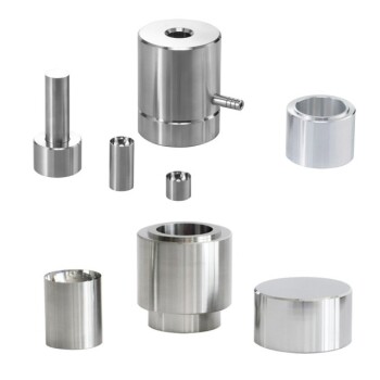
Related Products
- Chemical Vapor Deposition CVD Equipment System Chamber Slide PECVD Tube Furnace with Liquid Gasifier PECVD Machine
- RF PECVD System Radio Frequency Plasma-Enhanced Chemical Vapor Deposition RF PECVD
- Electron Beam Evaporation Coating Conductive Boron Nitride Crucible BN Crucible
- E Beam Crucibles Electron Gun Beam Crucible for Evaporation
- VHP Sterilization Equipment Hydrogen Peroxide H2O2 Space Sterilizer
People Also Ask
- What is the difference between thermal CVD and PECVD? Choose the Right Thin-Film Deposition Method
- What is the difference between CVD and PECVD? Choose the Right Thin-Film Deposition Method
- How is PECVD different from CVD? Unlock Low-Temperature Thin Film Deposition
- What is the difference between CVD and PVD process? A Guide to Choosing the Right Coating Method
- What are the advantages of PECVD over CVD? Achieve High-Quality Thin Films at Lower Temperatures