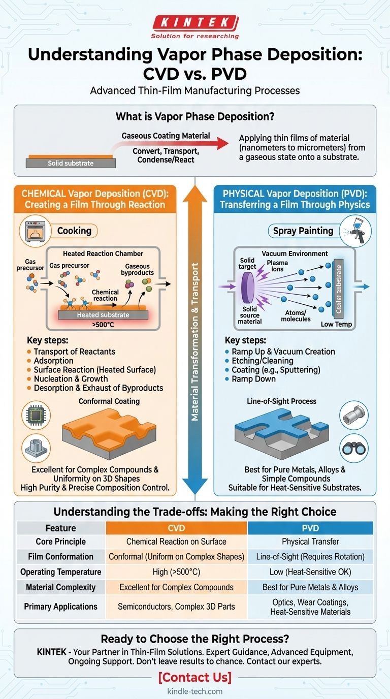
Vapor phase deposition is a family of advanced manufacturing processes used to apply very thin films of material onto a surface, known as a substrate. At its core, the process involves converting the coating material into a gaseous state, transporting it to the substrate, and then having it condense or react to form a solid layer. The two primary categories of this process are Chemical Vapor Deposition (CVD) and Physical Vapor Deposition (PVD).
The fundamental difference between vapor deposition processes lies in how the coating material arrives. Chemical Vapor Deposition (CVD) uses chemical reactions on the substrate's surface to create the film, while Physical Vapor Deposition (PVD) physically transfers the source material onto the substrate without a chemical change.
Chemical Vapor Deposition (CVD): Creating a Film Through Reaction
CVD is analogous to cooking. You introduce specific gaseous ingredients (precursors) into a heated chamber, and they react on the surface of your substrate to "bake" a new, solid material onto it.
The Core Principle: A Chemical Reaction
In CVD, the material being deposited is not the same material that is introduced into the chamber. Instead, one or more volatile precursor gases are used.
A chemical reaction, typically activated by high temperature, occurs directly on the substrate's surface. This reaction forms the desired solid film and gaseous byproducts, which are then removed.
The Detailed CVD Process Steps
The CVD process is a highly controlled sequence of events that ensures a uniform and high-quality film.
- Transport of Reactants: The precursor gases are transported into the reaction chamber.
- Adsorption: The gas molecules stick to the substrate surface.
- Surface Reaction: The adsorbed molecules undergo a chemical reaction, catalyzed by the heated surface, to form the solid film material.
- Nucleation and Growth: The newly formed solid material creates initial sites (nucleation) and then builds up layer by layer to form the film.
- Desorption of Byproducts: The unwanted gaseous byproducts from the reaction detach from the surface.
- Transport of Byproducts: An exhaust system removes these gaseous byproducts from the chamber.
Physical Vapor Deposition (PVD): Transferring a Film Through Physics
PVD is more like spray painting, but on an atomic level. You take a solid source material, turn it into a vapor, and it travels in a straight line to coat whatever is in its path. All of this occurs within a high-vacuum environment.
The Core Principle: A Physical Transfer
In PVD, the source material is the same as the final coating material. The process physically liberates atoms or molecules from a solid source and transports them through a vacuum to the substrate.
There is no chemical reaction to create the film. The vaporized material simply condenses on the cooler substrate, forming the solid coating.
Example Process: Sputtering Deposition
Sputtering is a common PVD technique that provides a clear example of the physical transfer process.
- Ramp Up: The chamber is sealed and a vacuum is created to remove contaminants. The environment is prepared, often by heating.
- Etching: The substrate is often cleaned using an ion bombardment process (cathodic cleaning) to ensure the surface is pure and the film will adhere properly.
- Coating: A high voltage is used to create a plasma. Ions from this plasma are accelerated and collide with the source material (the "target"), knocking off atoms. These ejected atoms travel through the vacuum and deposit onto the substrate.
- Ramp Down: Once the desired thickness is achieved, the system is safely returned to ambient temperature and pressure.
Understanding the Trade-offs: CVD vs. PVD
Choosing between these methods depends entirely on the material, the substrate, and the desired properties of the final film.
Film Conformance and Coverage
CVD excels at creating conformal coatings, meaning the film has a uniform thickness even over complex, three-dimensional shapes. The precursor gases can penetrate into trenches and around sharp corners before reacting.
PVD is a line-of-sight process. The vaporized atoms travel in a straight line, making it difficult to uniformly coat complex geometries without sophisticated substrate rotation.
Operating Temperature
CVD processes often require very high temperatures to drive the necessary chemical reactions. This can limit the types of substrates that can be coated without being damaged.
PVD can generally be performed at much lower temperatures, making it suitable for heat-sensitive materials like plastics or certain alloys.
Material Purity and Complexity
CVD offers exquisite control over the chemical composition (stoichiometry) of the film by precisely managing the flow of precursor gases. This is critical for creating the ultra-pure, complex compound films used in the semiconductor industry.
PVD is excellent for depositing pure metals, alloys, and certain simple compounds. Creating complex compound films can be more challenging than with CVD.
Making the Right Choice for Your Goal
To select the appropriate process, you must first define your most critical outcome.
- If your primary focus is coating complex, non-flat surfaces uniformly: CVD is often the superior choice due to the nature of gas-phase reactions.
- If your primary focus is depositing a pure metal or simple alloy onto a heat-sensitive substrate: PVD methods like sputtering are generally more suitable and operate at lower temperatures.
- If your primary focus is creating a highly pure, crystalline compound film for electronics: CVD offers the precise chemical control necessary for advanced semiconductor applications.
Understanding this core distinction between a film being chemically "created" versus physically "transferred" is the key to selecting the correct deposition technology for your project.
Summary Table:
| Feature | Chemical Vapor Deposition (CVD) | Physical Vapor Deposition (PVD) |
|---|---|---|
| Core Principle | Chemical reaction on substrate surface | Physical transfer of source material |
| Film Conformation | Conformal (uniform on complex shapes) | Line-of-sight (requires rotation for uniformity) |
| Operating Temperature | High (often > 500°C) | Low (suitable for heat-sensitive substrates) |
| Material Complexity | Excellent for complex compounds | Best for pure metals, alloys, and simple compounds |
| Primary Applications | Semiconductors, complex 3D parts | Optics, wear-resistant coatings, heat-sensitive materials |
Ready to Choose the Right Deposition Process for Your Lab?
Understanding the nuances between CVD and PVD is critical for achieving optimal thin-film results. KINTEK, your trusted partner in laboratory equipment, specializes in providing advanced vapor phase deposition solutions tailored to your specific research and production needs.
Whether you require the conformal coatings of CVD for complex semiconductor applications or the precision of PVD for heat-sensitive substrates, our experts can help you select and implement the perfect system.
Let KINTEK enhance your capabilities:
- Expert Guidance: Get personalized recommendations based on your material, substrate, and performance requirements.
- Advanced Equipment: Access state-of-the-art CVD and PVD systems from leading manufacturers.
- Ongoing Support: Benefit from installation, training, and maintenance services to ensure peak performance.
Don't leave your coating results to chance. Contact our experts today to discuss how KINTEK's vapor phase deposition solutions can drive your project's success!
Visual Guide
Related Products
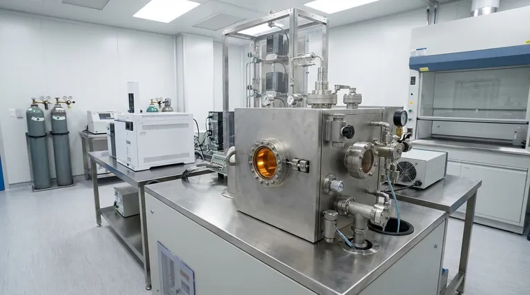
- Chemical Vapor Deposition CVD Equipment System Chamber Slide PECVD Tube Furnace with Liquid Gasifier PECVD Machine
- Customer Made Versatile CVD Tube Furnace Chemical Vapor Deposition Chamber System Equipment
- Microwave Plasma Chemical Vapor Deposition MPCVD Machine System Reactor for Lab and Diamond Growth
- 915MHz MPCVD Diamond Machine Microwave Plasma Chemical Vapor Deposition System Reactor
- Custom CVD Diamond Coating for Lab Applications
People Also Ask
- Why is Chemical Vapor Deposition (CVD) equipment uniquely suited for constructing hierarchical superhydrophobic structures?
- What are the advantages of chemical vapor deposition? Achieve Superior Thin Films for Your Lab
- What is plasma enhanced chemical vapor deposition PECVD equipment? A Guide to Low-Temperature Thin Film Deposition
- What are the core advantages of PE-CVD in OLED encapsulation? Protect Sensitive Layers with Low-Temp Film Deposition
- What is the chemical vapor deposition growth process? Build Superior Thin Films from the Atom Up


