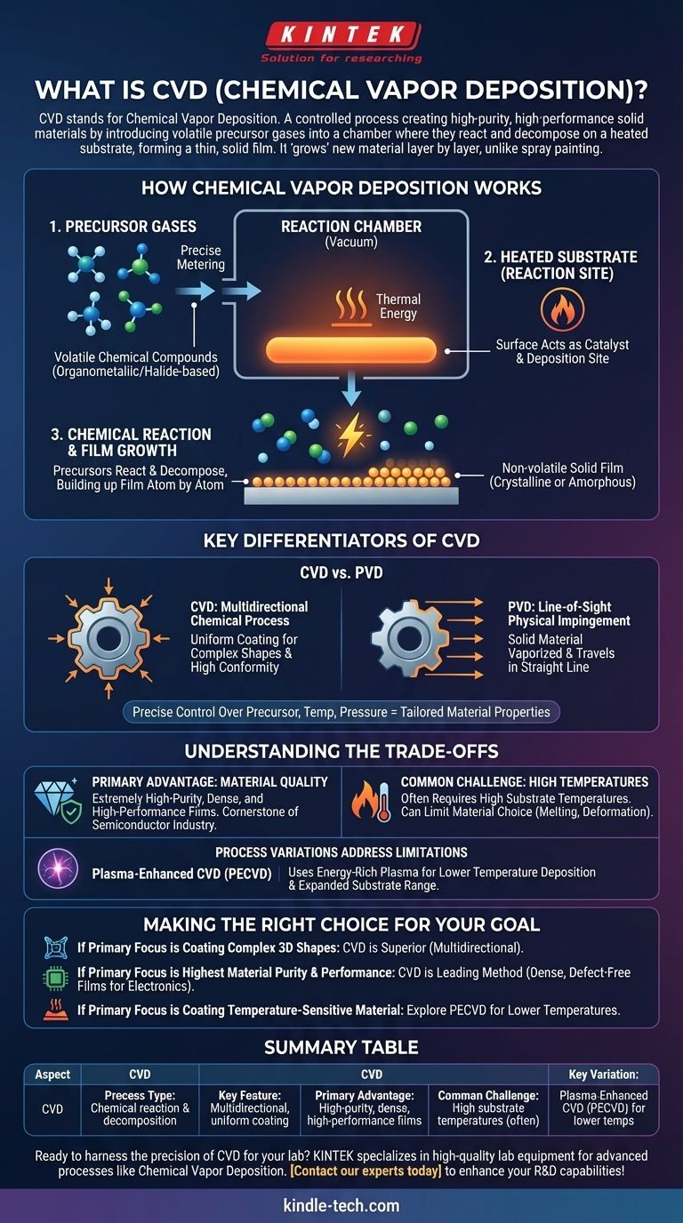
In the context of material science and manufacturing, CVD stands for Chemical Vapor Deposition. This is a highly controlled process used to create high-purity, high-performance solid materials. At its core, CVD involves introducing volatile precursor gases into a chamber where they react and decompose on a heated surface (the substrate), forming a thin, solid film.
Unlike a physical coating process like spray painting, Chemical Vapor Deposition uses a controlled chemical reaction to "grow" a new material layer by layer directly onto a surface. This chemical foundation is the key to producing the exceptionally pure and durable films the process is known for.
How Chemical Vapor Deposition Works
CVD is fundamentally a process of synthesis. You are not simply moving a material from one place to another; you are creating a new solid material from gaseous chemical ingredients.
The Role of Precursor Gases
The process begins with one or more volatile precursor gases. These are chemical compounds, often organometallic or halide-based, that contain the atoms you want to deposit.
These gases are precisely metered and fed into a reaction chamber, which is typically held under vacuum to prevent contamination.
The Heated Substrate as the Reaction Site
Inside the chamber is a substrate, which is the object or material that will be coated. This substrate is heated to a specific, high temperature.
The heat is not just for warming; it provides the critical thermal energy required to initiate the chemical reaction. The substrate's surface acts as the catalyst and deposition site.
The Chemical Reaction and Film Growth
As the precursor gases flow over the hot substrate, they react and/or decompose. This chemical change causes a new, non-volatile solid material to form.
This solid material deposits directly onto the substrate's surface, building up a thin film atom by atom or molecule by molecule. The resulting film can be crystalline or amorphous depending on the process conditions.
Key Differentiators of CVD
The "chemical" part of Chemical Vapor Deposition is what distinguishes it from other deposition techniques.
CVD vs. PVD: Chemical Reaction vs. Physical Impingement
The most common comparison is with Physical Vapor Deposition (PVD). PVD is a "line-of-sight" process where a solid material is vaporized (e.g., by sputtering) and then travels in a straight line to condense on the substrate.
CVD, however, is a multidirectional chemical process. Because the deposition happens from a reactive gas that fills the chamber, it can uniformly coat complex, non-flat surfaces with high conformity.
Control Over Material Properties
By precisely adjusting the precursor gas composition, temperature, pressure, and flow rates, engineers can create films with a wide range of tailored physical, chemical, and tribological properties.
Understanding the Trade-offs
While powerful, CVD is not a universal solution. Understanding its limitations is key to using it effectively.
Primary Advantage: Material Quality
The main benefit of CVD is the ability to produce extremely high-purity, dense, and high-performance films. It is a cornerstone of the semiconductor industry for this reason.
Common Challenge: High Temperatures
Traditional CVD often requires very high substrate temperatures to drive the chemical reaction. This can limit the types of materials that can be coated, as some substrates may melt, deform, or be otherwise damaged by the heat.
Process Variations Address Limitations
To overcome the temperature challenge, variations have been developed. Plasma-Enhanced CVD (PECVD), for example, uses an energy-rich plasma to help drive the chemical reaction.
This allows deposition to occur at much lower temperatures, expanding the range of compatible substrates without sacrificing many of the benefits.
Making the Right Choice for Your Goal
Understanding the core principles of CVD allows you to identify when it is the most appropriate manufacturing tool.
- If your primary focus is coating complex 3D shapes with a uniform layer: CVD is often superior to line-of-sight methods due to its chemical, non-directional nature.
- If your primary focus is achieving the highest material purity and performance: CVD is a leading method for producing dense, defect-free films for demanding applications like electronics and wear-resistant coatings.
- If your primary focus is coating a temperature-sensitive material: You should explore lower-temperature variations like PECVD to prevent damage to the underlying substrate.
Ultimately, CVD is a foundational technique for creating materials from the atom up, offering a level of control and quality that purely physical processes cannot match.
Summary Table:
| Aspect | CVD (Chemical Vapor Deposition) |
|---|---|
| Process Type | Chemical reaction & decomposition |
| Key Feature | Multidirectional, uniform coating |
| Primary Advantage | High-purity, dense, high-performance films |
| Common Challenge | High substrate temperatures (often) |
| Key Variation | Plasma-Enhanced CVD (PECVD) for lower temps |
Ready to harness the precision of CVD for your lab? KINTEK specializes in providing high-quality lab equipment and consumables tailored for advanced processes like Chemical Vapor Deposition. Whether you need to coat complex 3D shapes or achieve the highest material purity, our solutions are designed to meet your specific laboratory needs. Contact our experts today to discuss how we can enhance your research and development capabilities!
Visual Guide
Related Products
- CVD Diamond Dressing Tools for Precision Applications
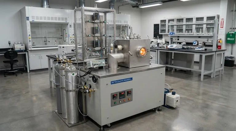
- Multi Heating Zones CVD Tube Furnace Machine Chemical Vapor Deposition Chamber System Equipment
- CVD Diamond Domes for Industrial and Scientific Applications
- CVD Diamond for Thermal Management Applications
- Chemical Vapor Deposition CVD Equipment System Chamber Slide PECVD Tube Furnace with Liquid Gasifier PECVD Machine
People Also Ask
- Can CVD diamonds change color? No, their color is permanent and stable.
- What are the disadvantages of CVD diamonds? Understanding the trade-offs for your purchase.
- Does the chemical vapor deposition be used for diamonds? Yes, for Growing High-Purity Lab Diamonds
- How long does it take to make synthetic diamonds? Discover the 6-8 Week Science Behind Lab-Grown Gems
- How do you identify a CVD diamond? The Definitive Guide to Lab-Grown Diamond Verification


