At its core, Metal-Organic Chemical Vapor Deposition (MOCVD) is a highly precise manufacturing process used to grow ultra-thin, high-purity crystalline films. It is a specialized form of Chemical Vapor Deposition (CVD), where precursor gases react in a chamber to deposit a solid layer onto a substrate. The key distinction of MOCVD lies in its use of "metal-organic" precursors—complex molecules containing both metal and organic carbon-based elements—which are essential for fabricating modern high-performance electronic and photonic devices.
The fundamental difference of MOCVD is not the deposition process itself, but the specific metal-organic precursors it uses. This choice enables the atomic-level control required to build the complex, layered crystal structures that power devices like LEDs, lasers, and high-frequency transistors.
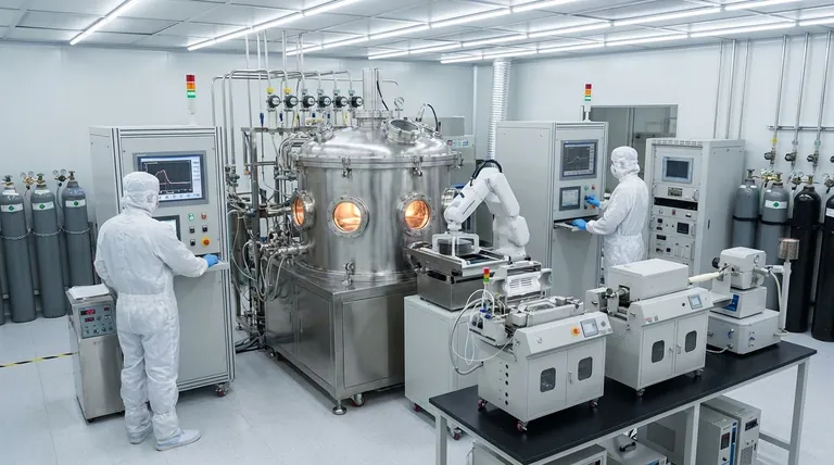
The Fundamentals of Chemical Vapor Deposition
To understand MOCVD, we must first understand the general principles of Chemical Vapor Deposition (CVD). It is a process that builds a solid material, typically a thin film, from a chemical reaction in a gaseous state.
The Reaction Chamber and Substrate
The entire process takes place inside a sealed reaction chamber under a controlled vacuum. The object to be coated, known as the substrate (such as a silicon wafer), is placed inside this chamber and heated to a specific temperature.
Introducing Precursor Gases
One or more volatile gases, known as precursors, are introduced into the chamber. These gases contain the chemical elements required to form the final film. The vacuum environment ensures purity and helps transport the precursor gases to the substrate surface.
The Deposition Reaction
When the hot precursor gases reach the surface of the substrate, the high temperature triggers a chemical reaction. The precursors decompose, leaving behind the desired solid material, which bonds to and forms a thin film on the substrate. Over time, this film grows layer by layer.
What Makes MOCVD a Specialized Process?
MOCVD operates on the same principles as general CVD but employs a specific class of precursors that give it unique capabilities.
The Role of Metal-Organic Precursors
The defining feature of MOCVD is its use of metal-organic source materials. These are molecules where a central metal atom is bonded to organic groups. For example, to create Gallium Nitride (GaN), a common MOCVD process might use Trimethylgallium (TMGa) as the metal-organic precursor for gallium and ammonia (NH₃) as the nitrogen source.
Achieving Crystalline Growth (Epitaxy)
MOCVD excels at epitaxy, which is the growth of a crystalline film on top of a crystalline substrate. Because the precursors deliver elements in a highly controlled way, the deposited atoms can arrange themselves to match the underlying crystal structure of the substrate, creating a perfect, single-crystal film.
Precision Control of Composition and Thickness
By precisely managing the flow rates of different precursor gases, engineers can control the composition of the film with atomic-level accuracy. This allows for the creation of heterostructures—stacks of different material layers, each only a few atoms thick—which are the building blocks of modern semiconductor devices.
Understanding the Trade-offs and Challenges
While powerful, MOCVD is not a universal solution. Its specialization comes with significant trade-offs.
Precursor Toxicity and Safety
Metal-organic precursors are often highly toxic and pyrophoric, meaning they can ignite spontaneously upon contact with air. This requires extremely sophisticated gas handling systems and safety protocols, adding significant complexity and cost to MOCVD equipment.
High Cost and Complexity
The need for high-purity precursors, complex vacuum and gas-flow systems, and uniform heating makes MOCVD a very expensive process. It is generally reserved for applications where the material quality justifies the investment.
Potential for Carbon Impurities
A key challenge in MOCVD is preventing carbon from the organic part of the precursor from being incorporated into the growing film as an impurity. This unwanted carbon can degrade the electronic or optical performance of the final device.
Key Applications Driven by MOCVD
MOCVD's ability to create high-quality compound semiconductors makes it the backbone of the optoelectronics industry.
Light-Emitting Diodes (LEDs)
The multi-layered quantum well structures inside high-brightness LEDs, especially blue, green, and white ones, are almost exclusively grown using MOCVD. The process allows for the precise tuning of material compositions to produce specific colors of light efficiently.
Semiconductor Lasers and Photodetectors
The lasers that power fiber-optic communications, data storage (like Blu-ray discs), and facial recognition sensors rely on the complex, atomically thin layers created by MOCVD.
High-Power and High-Frequency Electronics
Materials like Gallium Nitride (GaN) and Gallium Arsenide (GaAs), grown via MOCVD, are crucial for creating next-generation transistors. These are used in efficient power supplies, electric vehicles, and 5G cellular communication infrastructure.
Making the Right Choice for Your Goal
The decision to use MOCVD is driven entirely by the required material properties and the device's performance targets.
- If your primary focus is creating high-performance optoelectronics (like LEDs or lasers): MOCVD is the industry-standard method due to its unparalleled control over crystalline quality and complex layered structures.
- If your primary focus is depositing simple protective coatings (e.g., for corrosion or wear): A more general CVD or Physical Vapor Deposition (PVD) process is typically far more cost-effective and sufficient.
- If your primary focus is the research and development of novel compound semiconductors: MOCVD provides the essential flexibility to build and test complex heterostructures at the atomic scale.
Ultimately, understanding the unique role of its specialized precursors is the key to recognizing where MOCVD provides an indispensable manufacturing advantage.
Summary Table:
| Feature | Description |
|---|---|
| Core Principle | Chemical vapor deposition using metal-organic precursors for atomic-level control. |
| Key Differentiator | Use of metal-organic precursors (e.g., Trimethylgallium) enabling complex crystalline growth (epitaxy). |
| Primary Applications | Manufacturing of LEDs, semiconductor lasers, photodetectors, and high-frequency/power electronics. |
| Main Challenges | High cost, precursor toxicity, and potential for carbon impurities in the film. |
Ready to Integrate MOCVD Technology into Your Lab?
KINTEK specializes in providing advanced lab equipment and consumables for cutting-edge research and production. Whether you are developing next-generation semiconductors or optimizing your thin-film processes, our expertise and high-quality solutions are designed to meet your specific laboratory needs.
Contact us today to discuss how we can support your MOCVD applications and enhance your research capabilities.
Visual Guide

Related Products
- 915MHz MPCVD Diamond Machine Microwave Plasma Chemical Vapor Deposition System Reactor
- Multi Heating Zones CVD Tube Furnace Machine Chemical Vapor Deposition Chamber System Equipment
- Microwave Plasma Chemical Vapor Deposition MPCVD Machine System Reactor for Lab and Diamond Growth
- Cylindrical Resonator MPCVD Machine System Reactor for Microwave Plasma Chemical Vapor Deposition and Lab Diamond Growth
- Customer Made Versatile CVD Tube Furnace Chemical Vapor Deposition Chamber System Equipment
People Also Ask
- What is microwave plasma CVD? A Guide to High-Purity Diamond and Material Synthesis
- How is a diamond formed from CVD? The Science of Growing Diamonds Atom by Atom
- What pressure is needed for chemical vapor deposition of diamonds? Master the Low-Pressure 'Sweet Spot'
- How are CVD diamonds created? Discover the Science of Lab-Grown Diamond Precision
- What are the primary advantages of the CVD method for growing diamonds? Engineering High-Purity Gems and Components


