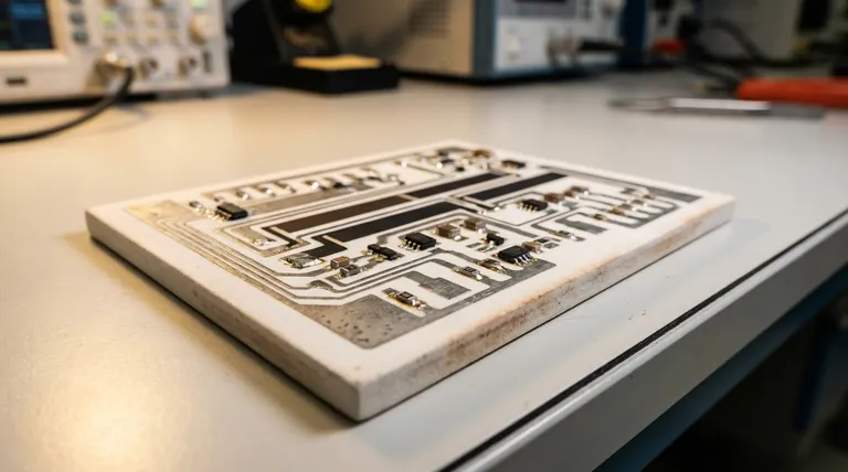
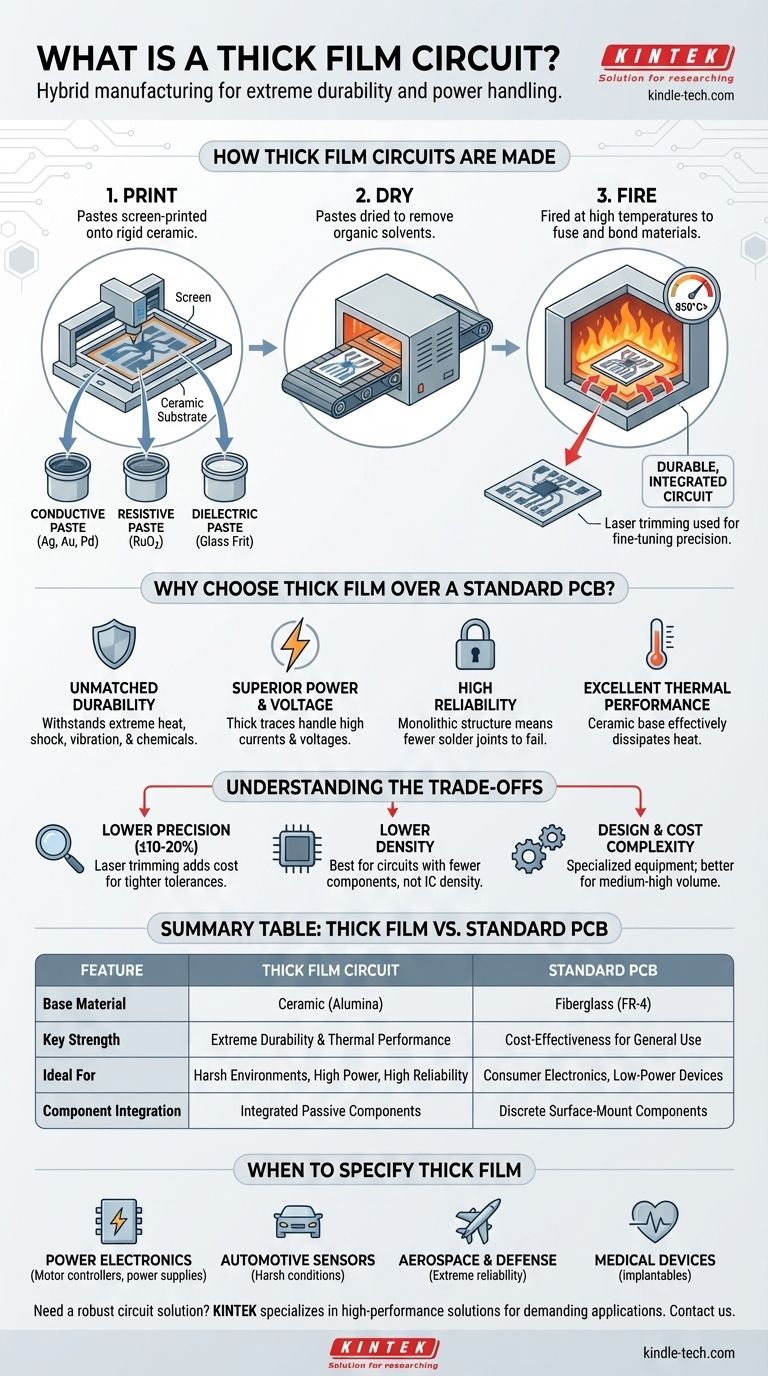
At its core, a thick film circuit is a method of manufacturing electronics where special conductive, resistive, and insulating "pastes" are screen-printed onto a rigid, heat-resistant substrate, typically made of ceramic. After printing, these layers are fired in a high-temperature furnace, fusing the materials to the substrate to create a durable, integrated circuit. This process directly forms passive components like resistors and capacitors on the substrate itself.
The central concept to grasp is that thick film technology is a hybrid manufacturing process. It bridges the gap between standard Printed Circuit Boards (PCBs) and monolithic Integrated Circuits (ICs), offering extreme durability and power handling where conventional electronics would fail.
How Thick Film Circuits Are Made
The manufacturing process is methodical and is what gives thick film its unique characteristics. It resembles screen-printing a design onto a t-shirt, but with functional electronic materials fired at over 850°C.
The Substrate: A Solid Foundation
The base of the circuit is almost always a ceramic substrate, most commonly alumina (aluminum oxide).
Unlike the fiberglass material (FR-4) of a standard PCB, ceramic offers superior thermal conductivity and is exceptionally stable at extreme temperatures.
The "Inks": Functional Pastes
The "inks" are actually viscous pastes containing fine particles of specific materials suspended in a glass frit and organic solvent.
There are three primary types:
- Conductive Pastes: Contain metals like silver, gold, or palladium to create circuit traces and connection pads.
- Resistive Pastes: Contain materials like ruthenium oxide to create integrated resistors. The specific composition determines the resistance.
- Dielectric Pastes: Are essentially glass-based insulators used to separate conductive layers or create the dielectric for integrated capacitors.
The Process: Print, Dry, and Fire
The circuit is built layer by layer. A patterned screen is used to print a paste onto the substrate, which is then dried in an oven to remove the solvents.
After all layers are printed and dried, the entire substrate is passed through a high-temperature kiln. This firing process burns off the organic binders and fuses the glass frit, permanently bonding the electronic materials to the ceramic.
For high-precision applications, resistors printed on the board are often fine-tuned using a high-energy beam in a process called laser trimming.
Why Choose Thick Film Over a Standard PCB?
While PCBs are ubiquitous, thick film technology excels in applications where the operating conditions are too demanding for standard organic materials.
Unmatched Durability and Thermal Performance
The ceramic substrate and fired components are inherently robust. They can withstand extreme temperatures, thermal shock, high vibration, and harsh chemical exposure far better than a PCB.
Ceramic's ability to dissipate heat makes thick film ideal for high-power electronics where thermal management is critical.
Superior Power and Voltage Handling
Thick film circuits can be designed with wider and thicker conductive traces, enabling them to handle significantly higher currents and voltages than PCBs of a similar size. This makes them a go-to choice for power electronics.
High Reliability in Harsh Environments
Because the components are fused into the substrate, there are fewer solder joints to fail. This monolithic structure results in exceptional long-term stability and reliability.
This is why thick film is dominant in automotive sensors, aerospace controls, and medical implantable devices where failure is not an option.
Understanding the Trade-offs
No technology is perfect. Thick film's strengths in durability come with compromises in other areas.
Precision and Tolerances
Thick film components, as-fired, have wider tolerances (often ±10-20%) than their discrete counterparts. Achieving high precision requires the extra step of laser trimming, which adds cost.
For applications demanding the tightest possible tolerances and finest features, thin film technology—a more precise but costly deposition process—is the superior choice.
Size and Component Density
While thick film integrates passive components, it cannot achieve the incredible density of a modern silicon Integrated Circuit (IC). It is best used for circuits with a moderate number of passive components and a few active (surface-mount) devices.
Design and Prototyping
Creating a thick film circuit requires specialized design knowledge and manufacturing equipment. The tooling and setup costs mean it is generally more economical for medium-to-high volume production runs rather than one-off prototypes.
When to Specify a Thick Film Circuit
Choosing the right technology depends entirely on the demands of your application.
- If your primary focus is high-power applications: Thick film is the ideal choice for motor controllers, power supplies, and high-power LED modules due to its thermal and current-handling capabilities.
- If your primary focus is extreme reliability in harsh environments: Specify thick film for automotive sensors, downhole drilling equipment, aerospace systems, or medical devices where failure rates must be near zero.
- If your primary focus is compact, general-purpose electronics: A standard PCB is almost always the more cost-effective and faster solution for consumer electronics, computers, and low-power devices.
- If your primary focus is high-frequency performance and ultimate precision: Thin film circuits offer better performance and tighter tolerances for RF, microwave, and high-precision instrumentation.
Ultimately, selecting thick film is a strategic decision to prioritize ruggedness and reliability over all other concerns.
Summary Table:
| Feature | Thick Film Circuit | Standard PCB |
|---|---|---|
| Base Material | Ceramic (e.g., Alumina) | Fiberglass (FR-4) |
| Key Strength | Extreme Durability & Thermal Performance | Cost-Effectiveness for General Use |
| Ideal For | Harsh Environments, High Power, High Reliability | Consumer Electronics, Low-Power Devices |
| Component Integration | Integrated Passive Components (Resistors, Capacitors) | Primarily Discrete Surface-Mount Components |
Need a robust circuit solution for demanding conditions? KINTEK specializes in high-performance lab equipment and consumables. If your project requires the durability and reliability of thick film technology for applications in automotive, aerospace, medical, or power electronics, our expertise can help. Contact our team today to discuss how we can support your laboratory's specific needs with precision-engineered solutions.
Visual Guide
Related Products
- Optical Window Glass Substrate Wafer Quartz Plate JGS1 JGS2 JGS3
- Float Soda-Lime Optical Glass for Laboratory Use
- MgF2 Magnesium Fluoride Crystal Substrate Window for Optical Applications
- Laboratory CVD Boron Doped Diamond Materials
- Optical Window Glass Substrate Wafer Barium Fluoride BaF2 Substrate Window
People Also Ask
- What substrates are used for thin film deposition? Choosing the Right Foundation for Your Application
- What are the advantages of thin film substrate? Enhance Surface Functionality for Superior Products
- How is deposition time calculated? Mastering the Clock for Strategic Legal Advantage
- What is the principle of quenching effect? Harnessing Molecular Interactions to Control Fluorescence
- What is the purpose of laminating? Protect and Enhance Your Documents for Long-Term Use