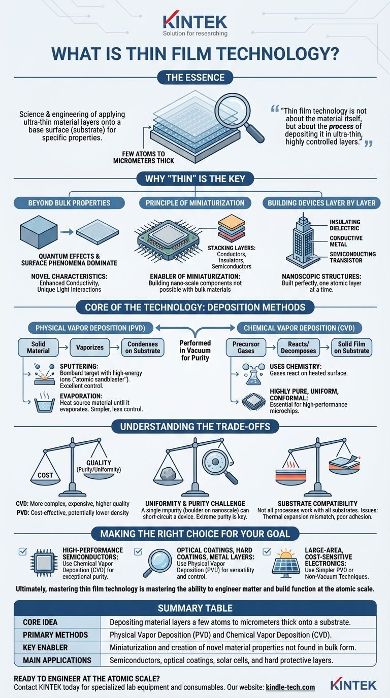
In essence, thin film technology is the science and engineering of applying material layers that are often only a few atoms to a few micrometers thick onto a base surface, known as a substrate. These films are the building blocks of virtually all modern electronics, from the processor in your phone to the anti-reflective coating on your glasses. The "technology" part refers to the highly precise processes used to deposit and pattern these layers to achieve specific electrical, optical, or mechanical properties.
The crucial insight is that thin film technology is not about the material itself, but about the process of depositing it in ultra-thin, highly controlled layers. This precision is what enables the miniaturization and advanced functionality of modern devices.
Why "Thin" Is the Key to Modern Technology
The shift from using materials in their bulk form to using them as thin films was not just an engineering choice; it was a fundamental necessity for technological progress.
Beyond Bulk Material Properties
A material's properties can change dramatically when it is reduced to a thin film. At this near-atomic scale, quantum effects and surface phenomena become dominant.
This allows engineers to create materials with novel characteristics, such as enhanced conductivity or unique light interactions, that are not present in the same material's bulk form.
The Principle of Miniaturization
Thin films are the primary enabler of miniaturization. You cannot build a billion-transistor computer chip, where components are measured in nanometers, using thick, bulk materials.
This technology allows for the stacking of different functional layers—conductors, insulators, and semiconductors—in a compact, vertical structure, which is the architectural basis of all integrated circuits.
Building Devices Layer by Layer
Think of manufacturing a microchip like constructing a skyscraper. Each thin film is a different floor, precisely laid down with a specific function.
One layer might be an insulating dielectric, the next a conductive metal pathway, and the next a semiconducting transistor channel. Thin film technology provides the tools to build this "nanoscopic" structure perfectly, one atomic layer at a time.
The Core of the Technology: Deposition Methods
The heart of thin film technology lies in its deposition processes, which are typically performed in a vacuum to ensure purity. These methods fall into two main categories.
Physical Vapor Deposition (PVD)
PVD involves physically transforming a solid material into a vapor, which then travels and condenses onto the substrate as a thin film.
Sputtering is a common PVD technique. In this process, a target made of the desired film material is bombarded with high-energy ions. This collision acts like an atomic-scale sandblaster, knocking atoms off the target that then coat the substrate. It offers excellent control and is widely used for metals and ceramics.
Evaporation is another PVD method where the source material is heated in a vacuum until it evaporates. The vapor then rises and condenses on the cooler substrate. It is simpler than sputtering but often provides less control over the film's structure.
Chemical Vapor Deposition (CVD)
CVD uses chemistry to build the film. Precursor gases are introduced into a reaction chamber containing the heated substrate.
The gases react or decompose on the hot surface, leaving behind a solid film of the desired material. CVD is renowned for producing highly pure, uniform, and conformal films, making it essential for high-performance semiconductor manufacturing.
Understanding the Trade-offs
Choosing a deposition method involves navigating a complex set of engineering and economic compromises. The "best" method is entirely dependent on the final application.
Cost vs. Quality
Generally, CVD processes are more complex and expensive to operate than PVD methods. However, they can produce films of unparalleled purity and uniformity, which is non-negotiable for cutting-edge microprocessors.
Simpler methods like thermal evaporation are cost-effective but may not be suitable for applications demanding high-density, defect-free films.
The Challenge of Uniformity and Purity
As devices shrink, the impact of a single atomic impurity or a slight variation in thickness is magnified. A microscopic dust particle can be a catastrophic "boulder" on the nanoscale, short-circuiting a device.
Maintaining extreme purity within the vacuum chamber and ensuring the film is deposited with perfect uniformity across the entire substrate are the greatest challenges in this field.
Substrate Compatibility
Not every deposition process works for every material or substrate. High-temperature CVD processes, for example, cannot be used on plastic substrates that would melt.
Furthermore, issues like thermal expansion mismatch and poor adhesion can cause the film to crack, peel, or delaminate, rendering the device useless.
Making the Right Choice for Your Goal
The ideal thin film method depends entirely on the application's specific requirements for performance, cost, and material type.
- If your primary focus is high-performance semiconductors: Chemical Vapor Deposition (CVD) and its advanced variants are often the standard due to their ability to create exceptionally pure and conformal layers.
- If your primary focus is optical coatings, hard coatings on tools, or metal layers: Physical Vapor Deposition (PVD) methods like sputtering offer excellent versatility, control, and efficiency for a wide range of materials.
- If your primary focus is large-area, cost-sensitive electronics like some solar cells: Simpler PVD methods or even non-vacuum, solution-based techniques may be the most economical choice.
Ultimately, mastering thin film technology is mastering the ability to engineer matter and build function at the atomic scale.
Summary Table:
| Key Aspect | Description |
|---|---|
| Core Idea | Depositing material layers a few atoms to micrometers thick onto a substrate. |
| Primary Methods | Physical Vapor Deposition (PVD) and Chemical Vapor Deposition (CVD). |
| Key Enabler | Miniaturization and creation of novel material properties not found in bulk form. |
| Main Applications | Semiconductors, optical coatings, solar cells, and hard protective layers. |
Ready to Engineer at the Atomic Scale?
Choosing the right thin film deposition process is critical to your project's success. Whether you require the high purity of CVD for semiconductor research or the versatility of PVD for advanced coatings, KINTEK has the expertise and equipment to meet your laboratory's specific needs.
Contact KINTEK today to discuss how our specialized lab equipment and consumables can help you master thin film technology and push the boundaries of innovation.
Visual Guide
Related Products
- HFCVD Machine System Equipment for Drawing Die Nano-Diamond Coating
- 915MHz MPCVD Diamond Machine Microwave Plasma Chemical Vapor Deposition System Reactor
- Vacuum Hot Press Furnace Machine for Lamination and Heating
- 1200℃ Split Tube Furnace with Quartz Tube Laboratory Tubular Furnace
- CVD Diamond Cutting Tool Blanks for Precision Machining
People Also Ask
- Is sputtering a PVD? Discover the Key Coating Technology for Your Lab
- What is the process of coating deposition? A Step-by-Step Guide to Thin Film Engineering
- What is microwave plasma CVD? A Guide to High-Purity Diamond and Material Synthesis
- How is something diamond coated? A Guide to CVD Growth vs. Plating Methods
- How do CVD diamonds grow? A Step-by-Step Guide to Lab-Grown Diamond Creation