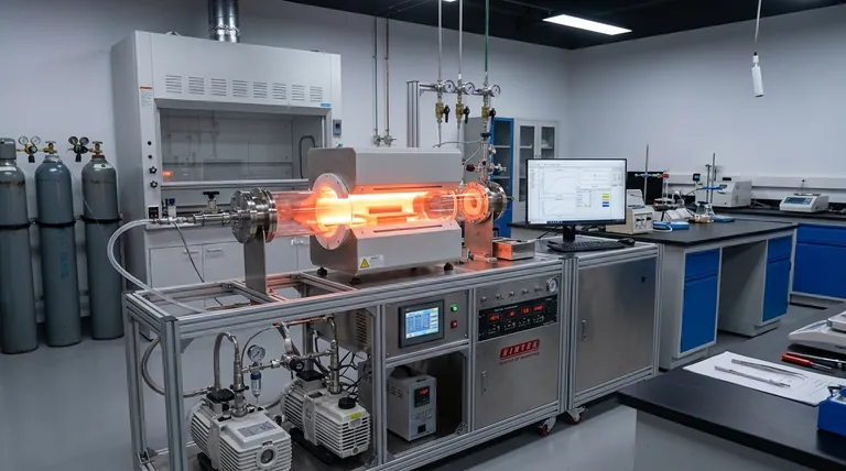
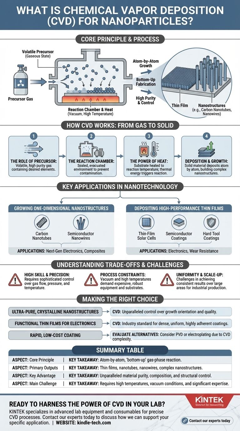
At its core, Chemical Vapor Deposition (CVD) is a synthesis process used to produce high-purity, high-performance solid materials. In this process, a substrate or part is placed in a reaction chamber and exposed to volatile precursor gases. When heated, these gases react or decompose on the substrate's surface, forming a solid deposit, which can be a thin film or a discrete nanostructure like a nanotube.
CVD is not merely a coating technique; it is a 'bottom-up' fabrication method that provides atomic-level control. By precisely managing precursor gases, temperature, and pressure, engineers can grow complex nanostructures or deposit exceptionally pure, high-performance films onto a surface.
How CVD Works: From Gas to Solid Nanostructure
Understanding the CVD process is about understanding a controlled chemical reaction. The entire process takes place within a sealed chamber, often under vacuum, to ensure purity and control.
The Role of the Precursor
A volatile precursor is the starting point. This is a chemical compound containing the elements you want to deposit, which has been converted into a gaseous state.
The choice of precursor is critical, as it dictates the composition and quality of the final material.
The Reaction Chamber
The substrate is placed inside a reaction chamber, which is then typically evacuated to create a vacuum. This removes unwanted contaminants that could interfere with the chemical reaction.
The precursor gases are then injected into this controlled environment.
The Power of Heat
The substrate is heated to a precise reaction temperature. This thermal energy is the catalyst that forces the precursor gas to either react with other gases or decompose.
This breakdown releases the desired elements, which are now ready to bond to the heated surface.
Deposition and Growth
As the precursor gas decomposes, the solid material is deposited atom by atom onto the substrate.
Over time, this process builds up a layer. Depending on the conditions, this can form a uniform, dense thin film or grow into specific shapes, such as nanowires or carbon nanotubes.
Key Applications in Nanotechnology
CVD is a foundational process in nanotechnology because of its precision. It enables the creation of materials with properties that are impossible to achieve through traditional bulk manufacturing.
Growing One-Dimensional Nanostructures
CVD is frequently the method of choice for growing 1D nanostructures.
It is renowned for producing high-quality carbon nanotubes and semiconductor nanowires (e.g., Gallium Nitride, GaN), which are critical components in next-generation electronics and composites.
Depositing High-Performance Thin Films
The process excels at depositing thin films with specific functions onto a wide range of materials, including metals, ceramics, and glass.
These applications include creating the active layers in thin-film solar cells, depositing insulating or conductive films on semiconductors, and forming exceptionally hard coatings on cutting tools to prevent wear and corrosion.
Understanding the Trade-offs and Challenges
While powerful, CVD is not a universally simple solution. Its precision comes with a set of operational requirements and limitations that must be considered.
Need for High Skill and Precision
CVD is a complex process that demands a high level of expertise. Controlling the gas flow, pressure, and temperature gradients requires sophisticated equipment and deep process knowledge to achieve repeatable results.
Process Constraints: Vacuum and High Temperatures
The requirement for a vacuum environment and high reaction temperatures means that the equipment can be expensive and energy-intensive.
Furthermore, the substrate material must be able to withstand the high temperatures involved without degrading or warping.
Uniformity and Scale-Up
Achieving a perfectly uniform coating or consistent nanostructure growth over a large surface area can be a significant challenge.
Scaling a successful lab-scale process to an industrial production level often requires extensive process optimization.
Making the Right Choice for Your Goal
Selecting CVD depends entirely on your material requirements and production constraints. Its value lies in its ability to produce high-purity materials with structural control.
- If your primary focus is creating ultra-pure, crystalline nanostructures (like nanowires or nanotubes): CVD offers unparalleled control over growth orientation and material quality, making it a superior choice.
- If your primary focus is applying a functional thin film for electronics or wear resistance: CVD is an industry-standard method for creating the dense, uniform, and highly adherent coatings required for high performance.
- If your primary focus is rapid, low-cost coating of simple geometries: You may need to evaluate CVD against other methods like Physical Vapor Deposition (PVD) or electroplating, as CVD's complexity can be a limiting factor.
Ultimately, mastering CVD is about harnessing controlled chemical reactions to build materials from the atom up.
Summary Table:
| Aspect | Key Takeaway |
|---|---|
| Core Principle | A 'bottom-up' fabrication method using gas-phase chemical reactions to deposit solid materials atom by atom. |
| Primary Outputs | Thin films, carbon nanotubes, semiconductor nanowires, and other complex nanostructures. |
| Key Advantage | Unparalleled control over material purity, composition, and structure. |
| Main Challenge | Requires high temperatures, vacuum conditions, and significant expertise for consistent results. |
Ready to harness the power of CVD in your lab?
KINTEK specializes in providing the advanced lab equipment and consumables needed for precise Chemical Vapor Deposition processes. Whether you are growing carbon nanotubes or depositing high-performance thin films, our solutions are designed to meet the rigorous demands of nanotechnology research and development.
Contact our experts today to discuss how we can support your specific application and help you achieve superior material synthesis results.
Visual Guide
Related Products
- Chemical Vapor Deposition CVD Equipment System Chamber Slide PECVD Tube Furnace with Liquid Gasifier PECVD Machine
- RF PECVD System Radio Frequency Plasma-Enhanced Chemical Vapor Deposition RF PECVD
- Microwave Plasma Chemical Vapor Deposition MPCVD Machine System Reactor for Lab and Diamond Growth
- Customer Made Versatile CVD Tube Furnace Chemical Vapor Deposition Chamber System Equipment
- 915MHz MPCVD Diamond Machine Microwave Plasma Chemical Vapor Deposition System Reactor
People Also Ask
- What happens during deposition chemistry? Building Thin Films from Gaseous Precursors
- What are the processes of vapor phase deposition? Understand CVD vs. PVD for Superior Thin Films
- How are carbon nanotubes grown? Master Scalable Production with Chemical Vapor Deposition
- What are the core advantages of PE-CVD in OLED encapsulation? Protect Sensitive Layers with Low-Temp Film Deposition
- What types of substrates are used in CVD to facilitate graphene films? Optimize Graphene Growth with the Right Catalyst


