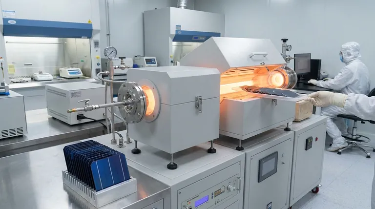
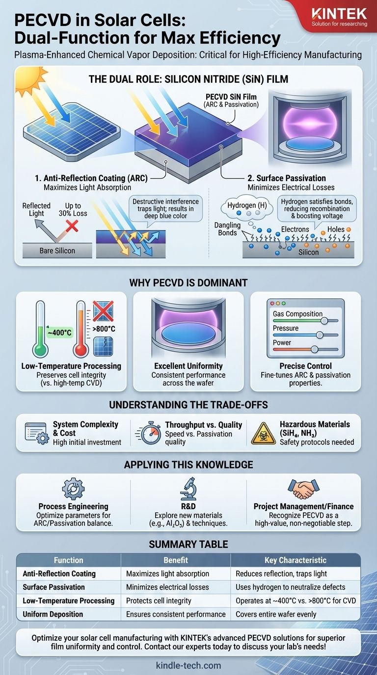
In solar cell manufacturing, PECVD is a critical process used to deposit a thin film of silicon nitride (SiN) onto the surface of a silicon wafer. This is not simply a protective layer; it serves a dual purpose that is essential for modern high-efficiency solar cells: it acts as both an anti-reflection coating to maximize light absorption and a passivation layer to minimize electrical losses.
A solar cell's performance is limited by two key factors: light reflecting off its surface instead of being absorbed, and electrical energy being lost at the surface before it can be collected. PECVD, or Plasma-Enhanced Chemical Vapor Deposition, is the industry-standard solution that addresses both of these problems simultaneously with a single, precisely engineered film.
The Dual Role of the PECVD Film
The film deposited by PECVD—typically silicon nitride—is responsible for a significant boost in solar cell efficiency. It accomplishes this by performing two separate functions at once.
Function 1: The Anti-Reflection Coating (ARC)
Bare, polished silicon is highly reflective, much like a mirror. It can reflect over 30% of the sunlight that hits it, which is a massive loss of potential energy.
PECVD deposits a film with a very specific thickness and refractive index. This film is engineered to cause destructive interference for light wavelengths that are most critical for power generation, effectively "trapping" more light inside the cell.
The distinct deep blue or purplish-black color of most modern solar panels is a direct visual result of this PECVD-deposited anti-reflection coating.
Function 2: Surface Passivation
The surface of a silicon wafer is an area of massive electrical imperfection. It contains countless incomplete chemical bonds, often called "dangling bonds."
These dangling bonds act as traps for the electrons that are generated when sunlight strikes the cell. If an electron gets trapped, it recombines and is lost before it can contribute to the electrical current. This process is a major source of efficiency loss.
The PECVD process incorporates hydrogen into the silicon nitride film. This hydrogen diffuses into the silicon surface and satisfies these dangling bonds, effectively "passivating" or electrically neutralizing them. This dramatically reduces electron loss and boosts the cell's voltage and current.
Why PECVD is the Dominant Technology
While other methods can deposit films, PECVD has a unique combination of advantages that make it ideal for mass-producing high-efficiency solar cells.
Low-Temperature Processing
Traditional Chemical Vapor Deposition (CVD) requires very high temperatures (often >800°C) to work. Such high temperatures would damage the sensitive electronic junctions that have already been created within the solar cell.
PECVD uses an energized plasma to break down the precursor gases (like silane and ammonia). This plasma provides the energy for the reaction, allowing high-quality films to be deposited at much lower temperatures (~400°C), preserving the integrity of the solar cell.
Excellent Uniformity and Coverage
The plasma process ensures the silicon nitride film is deposited with exceptional uniformity across the entire large surface area of the silicon wafer.
This consistency is critical for manufacturing, as it ensures that every part of the solar cell performs at the same high level, leading to a reliable and powerful final product.
Precise Control Over Film Properties
By adjusting the plasma parameters—such as gas composition, pressure, and power—manufacturers have fine-grained control over the final film.
They can precisely tune the refractive index to optimize the anti-reflection properties and control the film's density and hydrogen content to maximize the passivation effect. This tunability is key to pushing cell efficiencies ever higher.
Understanding the Trade-offs
Despite its advantages, PECVD is not without its complexities. Acknowledging them is key to understanding its place in the manufacturing line.
System Complexity and Cost
PECVD tools are sophisticated vacuum deposition systems. They represent a significant capital investment compared to simpler methods and require skilled personnel to operate and maintain.
Throughput vs. Quality
There is a constant engineering trade-off between the speed of deposition (manufacturing throughput) and the ultimate quality of the film. Running the process faster can sometimes result in a film with less effective passivation properties, requiring careful process optimization.
Hazardous Materials
The precursor gases used in the process, primarily silane (SiH₄) and ammonia (NH₃), are hazardous. Their use necessitates stringent safety protocols and infrastructure, adding to the operational complexity and cost.
Applying This Knowledge
Understanding PECVD's function allows you to better assess its role in the solar value chain.
- If your primary focus is process engineering or manufacturing: Your goal is to optimize PECVD parameters to co-optimize ARC and passivation properties, maximizing cell efficiency while maintaining high factory throughput.
- If your primary focus is R&D or materials science: You might explore new materials beyond SiN, such as aluminum oxide (Al₂O₃), or advanced PECVD techniques to achieve even lower levels of surface recombination for next-generation cells.
- If your primary focus is project management or finance: You should recognize the PECVD process step as a non-negotiable, high-value-add stage that directly determines the final power rating and bankability of the solar module.
Grasping PECVD's dual function is fundamental to understanding how a simple silicon wafer is transformed into a highly efficient device for generating clean electricity.
Summary Table:
| Function | Benefit | Key Characteristic |
|---|---|---|
| Anti-Reflection Coating | Maximizes light absorption | Reduces reflection, traps light |
| Surface Passivation | Minimizes electrical losses | Uses hydrogen to neutralize defects |
| Low-Temperature Processing | Protects cell integrity | Operates at ~400°C vs. >800°C for CVD |
| Uniform Deposition | Ensures consistent performance | Covers entire wafer evenly |
Optimize your solar cell manufacturing with KINTEK's advanced PECVD solutions. Our lab equipment and consumables are designed to help you achieve superior film uniformity, precise process control, and maximum efficiency for your solar cells. Whether you're in R&D or mass production, KINTEK provides the reliable tools you need to push the boundaries of performance. Contact our experts today to discuss how we can support your laboratory's specific needs!
Visual Guide
Related Products
- Chemical Vapor Deposition CVD Equipment System Chamber Slide PECVD Tube Furnace with Liquid Gasifier PECVD Machine
- RF PECVD System Radio Frequency Plasma-Enhanced Chemical Vapor Deposition RF PECVD
- Inclined Rotary Plasma Enhanced Chemical Vapor Deposition PECVD Equipment Tube Furnace Machine
- Inclined Rotary Plasma Enhanced Chemical Vapor Deposition PECVD Equipment Tube Furnace Machine
- 915MHz MPCVD Diamond Machine Microwave Plasma Chemical Vapor Deposition System Reactor
People Also Ask
- What happens during deposition chemistry? Building Thin Films from Gaseous Precursors
- How expensive is chemical vapor deposition? Understanding the True Cost of High-Performance Coating
- What are the advantages of chemical vapor deposition? Achieve Superior Thin Films for Your Lab
- How are carbon nanotubes grown? Master Scalable Production with Chemical Vapor Deposition
- What is the chemical vapor deposition growth process? Build Superior Thin Films from the Atom Up


