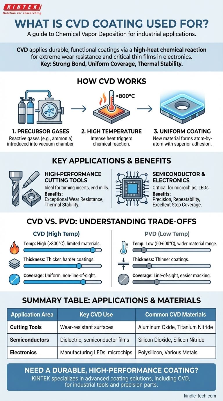
In short, Chemical Vapor Deposition (CVD) is used to apply highly durable, functional coatings onto materials for demanding industrial applications. Its primary uses are in creating extremely hard and wear-resistant surfaces for cutting tools and manufacturing critical thin films for the semiconductor and electronics industries.
The core principle of CVD is using a chemical reaction, triggered by high heat, to grow a new material layer directly onto a component's surface. This process creates an exceptionally strong bond and a uniform coating, making it ideal for applications demanding extreme hardness and thermal stability, but its high temperature limits the types of materials it can be used on.
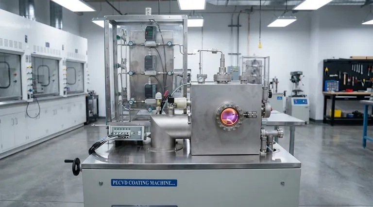
How Chemical Vapor Deposition (CVD) Works
CVD is fundamentally different from painting or plating. It doesn't just add a layer on top; it synthesizes a new material directly on the substrate through a chemical process.
The Role of Precursor Gases
The process begins by introducing specific reactive gases, known as precursors, into a vacuum chamber containing the part to be coated. For example, depositing silicon nitride requires gases like ammonia and dichlorosilane.
The Importance of High Temperature
These parts are heated to very high temperatures, often over 800°C (1472°F). This intense heat provides the energy needed to trigger a chemical reaction between the precursor gases.
Superior Adhesion and Uniform Coverage
The reaction causes a new, solid material to form and deposit atom-by-atom onto the hot surface, creating a thin film. Because this film is chemically bonded to the substrate, its adhesion is exceptionally strong.
Crucially, since the precursor gases surround the entire component, the coating forms uniformly over all exposed surfaces, including complex shapes and internal channels. This is a key advantage over "line-of-sight" processes.
Key Applications Driven by CVD's Properties
The unique characteristics of CVD—hardness, heat resistance, and uniform coverage—make it the superior choice for a specific set of high-performance applications.
High-Performance Cutting Tools
CVD is ideal for coating tools that experience continuous, high-stress cutting forces, such as turning inserts and some end mills or drill bits.
The thick (10-20 μm) and extremely hard coatings, often made of materials like aluminum oxide (Al2O3), provide exceptional wear resistance and thermal stability. This allows tools to maintain a sharp edge for longer when machining tough materials at high speeds.
Semiconductor and Electronics Manufacturing
CVD is a cornerstone technology in fabricating microchips, LEDs, solar cells, and other electronic devices. Its precision is essential for building microscopic structures layer by layer.
The process is used to deposit various critical films, including:
- Dielectric films (e.g., SiO₂, Si₃N₄) to insulate conductive layers.
- Semiconductor films that form the basis of transistors.
- Conductive metal films that create the circuits within a chip.
CVD's excellent repeatability and step coverage (its ability to coat the vertical walls of tiny trenches) are vital for the reliability and performance of modern electronics.
Understanding the Trade-offs: CVD vs. PVD
While both are vacuum deposition methods, CVD and Physical Vapor Deposition (PVD) have distinct advantages and limitations. Choosing between them depends entirely on the application's requirements.
Temperature: The Defining Limitation of CVD
The high temperatures required for the CVD process are its greatest strength and its biggest weakness. This heat limits its use to materials that can withstand it, such as cemented carbides, ceramics, and some high-temperature steels.
PVD, by contrast, operates at much lower temperatures (50-600°C), making it suitable for a wider range of materials, including heat-treated steels, plastics, and various alloys used in medical devices and consumer goods.
Coating Thickness and Hardness
CVD typically produces thicker, harder, and more abrasion-resistant coatings than PVD. This makes it superior for fighting the intense wear seen in continuous machining operations.
PVD coatings are thinner, which can be an advantage for preserving the sharpness of a highly precise cutting edge, making them ideal for tasks involving interrupted cuts like milling.
Coverage: Uniform vs. Line-of-Sight
CVD is a non-line-of-sight process. The reactive gas flows around the entire part, ensuring a uniform coating even on internal surfaces and complex geometries.
PVD is a line-of-sight process, where the coating material travels in a straight line from a source to the substrate. This makes it easier to mask off specific areas you don't want to coat but makes it challenging to cover complex or internal shapes.
Making the Right Choice for Your Application
Selecting the correct coating technology requires a clear understanding of your primary goal.
- If your primary focus is extreme wear and heat resistance: CVD is often the superior choice due to its thick, chemically bonded, and thermally stable coatings, ideal for heavy-duty industrial tooling.
- If your primary focus is coating heat-sensitive materials: PVD is the only viable option, as its low-temperature process will not damage or warp the underlying material.
- If your primary focus is uniformly coating complex internal geometries: CVD's non-line-of-sight nature gives it a distinct advantage for ensuring complete and even coverage.
- If your primary focus is aesthetic finishes or biocompatibility: PVD is the dominant technology for applications like fixtures, jewelry, and medical implants due to its versatility and lower process temperature.
By understanding these core principles, you can confidently select the coating technology that aligns perfectly with your material, geometry, and performance goals.
Summary Table:
| Application Area | Key CVD Coating Use | Common CVD Materials |
|---|---|---|
| Cutting Tools | Wear-resistant surfaces for inserts, end mills | Aluminum Oxide (Al₂O₃), Titanium Nitride (TiN) |
| Semiconductors | Dielectric, semiconductor, and conductive films | Silicon Dioxide (SiO₂), Silicon Nitride (Si₃N₄) |
| Electronics | Manufacturing of LEDs, solar cells, and microchips | Polysilicon, Various Metals |
Need a durable, high-performance coating for your components? KINTEK specializes in advanced coating solutions, including CVD, for industrial tools and precision parts. Our expertise ensures your products achieve superior wear resistance, thermal stability, and uniform coverage—even on complex geometries. Contact our coating experts today to discuss how we can enhance your product's performance and longevity.
Visual Guide
Related Products
- Custom CVD Diamond Coating for Lab Applications
- HFCVD Machine System Equipment for Drawing Die Nano-Diamond Coating
- Laboratory CVD Boron Doped Diamond Materials
- CVD Diamond Dressing Tools for Precision Applications
- CVD Diamond for Thermal Management Applications
People Also Ask
- What are the different CVD coating? A Guide to Thermal CVD, PECVD, and Specialized Methods
- What is CVD coated? A Guide to Superior Wear Resistance for Complex Parts
- What are the advantages of CVD coating? Superior Hardness and Uniformity for Demanding Applications
- What is the use of CVD coating? Enhance Durability and Functionality for Your Components
- How thick is CVD diamond coating? Balancing Durability and Stress for Optimal Performance


