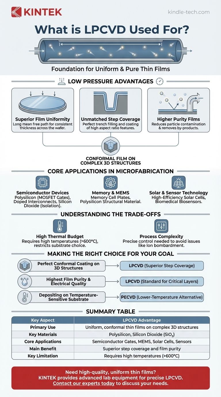
At its core, LPCVD is a foundational manufacturing process used to deposit exceptionally uniform and pure thin films, making it indispensable for creating modern semiconductor devices, MEMS, and solar cells. It excels at depositing critical materials like polysilicon and silicon dioxide, which form the building blocks of microelectronics.
Low-Pressure Chemical Vapor Deposition (LPCVD) is primarily used when the goal is to create a perfectly uniform, or conformal, film that covers every surface of a complex, three-dimensional microscopic structure with extreme precision.
Why Low Pressure is the Key Advantage
The defining characteristic of LPCVD is its operation in a vacuum (low-pressure) environment at high temperatures. This specific combination is not an arbitrary choice; it directly enables the unique qualities of the films it produces.
Superior Film Uniformity
Operating at low pressure significantly increases the mean free path of gas molecules in the reaction chamber. This means reactant molecules can travel farther and diffuse more freely before colliding.
The result is a deposition process that isn't limited by how fast the gas can reach the surface. Instead, it's governed by the surface reaction itself, leading to a highly consistent and uniform film thickness across the entire wafer.
Unmatched Step Coverage
This enhanced gas diffusion is critical for coating complex topographies. LPCVD excels at trench filling and coating features with a high aspect ratio (deep and narrow structures).
The process ensures that the bottom and sidewalls of a microscopic trench receive the same amount of deposited material as the top surface, creating a void-free, conformal layer essential for electrical isolation and device structure.
Higher Purity Films
LPCVD processes typically do not require an inert carrier gas to transport the reactive chemicals. Eliminating this extra gas reduces a potential source of particle contamination.
Furthermore, the low-pressure environment allows reaction by-products to be pumped out of the chamber quickly, preventing them from being incorporated into the growing film as impurities.
Core Applications in Microfabrication
The unique benefits of LPCVD make it the go-to method for depositing several critical films in high-volume manufacturing.
Semiconductor Devices
LPCVD is a workhorse in the semiconductor industry. It is used to deposit polysilicon, which forms the gate of a MOSFET—the fundamental switch in all modern computing.
Doped polysilicon is also used for electrical interconnects, while silicon dioxide films provide crucial electrical isolation between different components on a chip.
Memory and MEMS
In devices like DRAM, LPCVD is used to create films for memory cell plates.
It is also a dominant technology in producing Micro-Electro-Mechanical Systems (MEMS), where polysilicon serves as a primary structural material for microscopic sensors, actuators, and resonators.
Solar and Sensor Technology
The ability to produce high-quality, highly transparent films cost-effectively makes LPCVD valuable for manufacturing high-efficiency solar cells.
This same precision is leveraged in producing sensitive layers for biomedical devices, such as biosensors, and other complex sensor applications.
Understanding the Trade-offs
While powerful, LPCVD is not a universal solution. Its operating requirements create important limitations that must be considered.
High Thermal Budget
The most significant drawback of LPCVD is its reliance on high temperatures, often ranging from 600°C to over 900°C.
This high thermal budget restricts its use to substrates and previously deposited layers that can withstand the heat without degrading or diffusing. It is unsuitable for temperature-sensitive materials like polymers or certain metals.
Process Complexity
Achieving the desired film properties requires precise control over temperature, pressure, and gas flow.
Improper process parameters can lead to issues like increased ion bombardment, which may affect the final film quality and uniformity, especially during any associated etching steps.
Making the Right Choice for Your Goal
Selecting a deposition technique depends entirely on the required film properties and the constraints of your device.
- If your primary focus is perfect conformal coating on 3D structures: LPCVD is almost always the superior choice due to its excellent step coverage.
- If your primary focus is the highest possible film purity and electrical quality: LPCVD is the standard for critical layers like polysilicon gates and high-quality dielectrics.
- If your primary focus is depositing on a temperature-sensitive substrate: You must look to alternative, lower-temperature methods like Plasma-Enhanced CVD (PECVD).
Ultimately, LPCVD remains an essential tool precisely because it delivers a level of film quality and conformity that is difficult to achieve by any other means.
Summary Table:
| Key Aspect | LPCVD Advantage |
|---|---|
| Primary Use | Depositing uniform, conformal thin films on complex 3D structures |
| Key Materials | Polysilicon, Silicon Dioxide (SiO₂) |
| Core Applications | Semiconductor Gates, MEMS, Solar Cells, Sensors |
| Main Benefit | Superior step coverage and film purity |
| Key Limitation | Requires high temperatures (>600°C) |
Need high-quality, uniform thin films for your microfabrication process? KINTEK specializes in providing the advanced lab equipment and consumables essential for precise LPCVD and other deposition techniques. Our solutions help you achieve the exceptional film conformity and purity required for cutting-edge semiconductors, MEMS, and solar devices. Contact our experts today to discuss how we can support your specific laboratory needs.
Visual Guide
Related Products
- Inclined Rotary Plasma Enhanced Chemical Vapor Deposition PECVD Equipment Tube Furnace Machine
- Inclined Rotary Plasma Enhanced Chemical Vapor Deposition PECVD Equipment Tube Furnace Machine
- Chemical Vapor Deposition CVD Equipment System Chamber Slide PECVD Tube Furnace with Liquid Gasifier PECVD Machine
- Laboratory CVD Boron Doped Diamond Materials
- Microwave Plasma Chemical Vapor Deposition MPCVD Machine System Reactor for Lab and Diamond Growth
People Also Ask
- How does plasma enhance CVD? Unlock Low-Temperature, High-Quality Film Deposition
- What is plasma enhanced chemical vapour deposition PECVD used for? Enable Low-Temp Thin Films for Electronics & Solar
- What is the necessity of depositing a silicon nitride (SiNx) thin film using PECVD? Optimize QSSPC Lifetime Measurement
- How does the PECVD function enhance thin-film properties? Achieve Superior Chemical Stability & Durability
- How does plasma vapor deposition work? A Low-Temperature Coating Solution for Sensitive Materials


