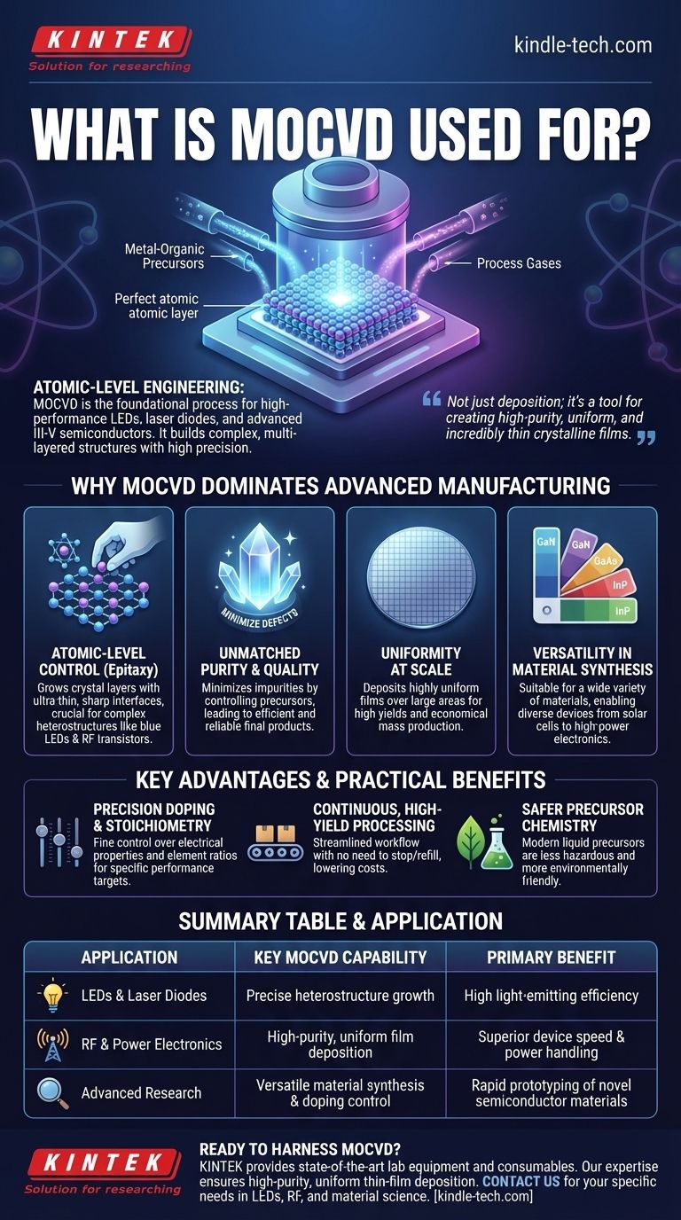
At its core, Metal Organic Chemical Vapor Deposition (MOCVD) is the foundational manufacturing process for high-performance LEDs, laser diodes, and advanced III-V semiconductors. It is the key technology used to build the complex, multi-layered structures required for modern radio frequency (RF) components and optoelectronics, particularly those based on materials like gallium nitride (GaN).
MOCVD isn't just a deposition method; it's a tool for atomic-level engineering. Its true value lies in its unparalleled precision, enabling the creation of the high-purity, uniform, and incredibly thin crystalline films that are the building blocks of today's most sophisticated electronic and photonic devices.
Why MOCVD Dominates Advanced Manufacturing
The reason MOCVD is so critical is that it offers a level of control that other methods struggle to match. It allows engineers to build complex semiconductor devices layer by atomic layer, which is essential for achieving high performance and efficiency.
The Principle of Atomic-Level Control
MOCVD is a form of epitaxy, which means growing a crystal layer on top of a crystalline substrate. This process allows for the creation of ultra-thin layers with extremely sharp and well-defined interfaces between different materials.
This precision is crucial for fabricating heterostructures, which are structures made of multiple different semiconductor materials stacked together. These complex stacks are what give devices like blue LEDs and high-frequency transistors their unique properties.
Ensuring Unmatched Purity and Quality
The performance of a semiconductor device is directly tied to the purity of its materials. The MOCVD process is engineered to grow high-purity crystalline compounds.
By carefully controlling the metal-organic chemical precursors and the reactor environment, manufacturers can minimize defects and impurities, leading to more efficient and reliable final products.
The Power of Uniformity at Scale
For any manufacturing process to be viable, it must be repeatable and scalable. MOCVD excels at depositing highly uniform films over large areas, such as an entire silicon wafer.
This uniformity ensures that every device produced from the wafer performs consistently, which is critical for achieving high yields and making large-scale production economically feasible.
Versatility in Material Synthesis
While MOCVD is famous for its use with GaN, its applications are much broader. The technique is suitable for growing a wide variety of materials and alloys.
This flexibility allows for the creation of diverse and highly specialized devices, from solar cells to high-power electronic components.
Understanding the Key Advantages
Beyond its core capabilities, MOCVD offers several practical advantages that have solidified its role in high-volume manufacturing. These benefits translate directly to better control, higher performance, and more efficient production.
Precision Doping and Stoichiometry
Doping involves intentionally introducing impurities into a semiconductor to alter its electrical properties. MOCVD provides exceptionally fine control over doping levels and distribution.
It also makes it easier to manage the stoichiometry, or the precise ratio of elements, within the deposited film. This control is fundamental to tuning a device for a specific performance target.
Continuous, High-Yield Processing
Modern MOCVD systems are designed for continuous operation. This means they do not need to be stopped and refilled during a deposition run, which streamlines the manufacturing workflow.
This continuous nature, combined with the high uniformity, contributes directly to higher production yields and lower costs for complex devices.
Advancements in Precursor Chemistry
Historically, some chemical precursors used in the process were highly toxic. However, modern MOCVD processes increasingly rely on liquid precursors that are significantly less hazardous and more environmentally friendly.
This shift has not only improved safety but also maintained the high quality and purity standards required for advanced electronics.
How to Apply This to Your Goal
Understanding the strengths of MOCVD helps you recognize where it is the indispensable choice. Your specific objective determines which of its capabilities is most critical.
- If your primary focus is manufacturing high-brightness LEDs or laser diodes: MOCVD's ability to precisely build complex GaN-based heterostructures is non-negotiable for achieving the required light-emitting efficiency.
- If your primary focus is developing high-speed RF or power electronics: The technology's capacity for creating high-purity, precisely doped layers is essential for maximizing device speed and power handling.
- If your primary focus is researching novel semiconductor materials: The versatility and fine-tuning capabilities of MOCVD make it an ideal platform for fabricating and testing experimental thin films and device structures with high precision.
Ultimately, MOCVD provides the foundational control needed to transform advanced material science into the high-performance devices that power our world.
Summary Table:
| Application | Key MOCVD Capability | Primary Benefit |
|---|---|---|
| LEDs & Laser Diodes | Precise heterostructure growth | High light-emitting efficiency |
| RF & Power Electronics | High-purity, uniform film deposition | Superior device speed & power handling |
| Advanced Research | Versatile material synthesis & doping control | Rapid prototyping of novel semiconductor materials |
Ready to harness the power of MOCVD for your advanced semiconductor projects? KINTEK specializes in providing state-of-the-art lab equipment and consumables for semiconductor manufacturing and research. Our expertise ensures you have the precise tools needed for high-purity, uniform thin-film deposition. Contact our experts today to discuss how we can support your laboratory's specific needs in LEDs, RF components, and material science.
Visual Guide
Related Products
- 915MHz MPCVD Diamond Machine Microwave Plasma Chemical Vapor Deposition System Reactor
- Multi Heating Zones CVD Tube Furnace Machine Chemical Vapor Deposition Chamber System Equipment
- Microwave Plasma Chemical Vapor Deposition MPCVD Machine System Reactor for Lab and Diamond Growth
- Cylindrical Resonator MPCVD Machine System Reactor for Microwave Plasma Chemical Vapor Deposition and Lab Diamond Growth
- Customer Made Versatile CVD Tube Furnace Chemical Vapor Deposition Chamber System Equipment
People Also Ask
- What are the primary advantages of the CVD method for growing diamonds? Engineering High-Purity Gems and Components
- What are the advantages of a Microwave Plasma CVD reactor for MCD/NCD coatings? Precision Multilayer Diamond Engineering
- How is a diamond formed from CVD? The Science of Growing Diamonds Atom by Atom
- Why is MW-CVD preferred for high-purity diamond optical windows? Achieve Zero-Contamination Material Growth
- What is microwave plasma CVD? A Guide to High-Purity Diamond and Material Synthesis


