Plasma-enhanced Chemical Vapor Deposition (PECVD) is a deposition technique that utilizes plasma energy, rather than strictly thermal energy, to initiate chemical reactions for forming thin films. By applying an electric field to create a highly reactive environment of ionized gas, PECVD facilitates deposition at significantly lower temperatures than conventional methods. This is a critical advantage in CMOS fabrication, where processing heat-sensitive substrates without damaging underlying structures is essential.
PECVD bridges the gap between high-quality film deposition and strict thermal budgets. By replacing thermal activation with plasma excitation, it enables the creation of uniform, durable films on delicate substrates that would otherwise be degraded by high-heat processes.
The Mechanism of Plasma Activation
Energy via Ionization
In standard Chemical Vapor Deposition (CVD), high heat is required to break chemical bonds and drive reactions. PECVD replaces this heat by using an electric field to ionize precursor gas molecules. This transforms the gas into a plasma state rich in active ions.
Lowering the Activation Barrier
The high internal energy of the plasma effectively fragments vapor phase precursors. This provides the necessary activation energy to initiate chemical reactions on the substrate surface. Consequently, the process can induce chemical changes that are difficult or impossible to achieve through thermal energy alone.
Critical Advantages for CMOS Fabrication
Reduced Thermal Budget
The most significant benefit of PECVD for CMOS is the ability to operate at lower substrate temperatures. This reduction in heat minimizes thermal stress on the wafer. It allows for the deposition of layers over temperature-sensitive materials without degrading previously fabricated components.
Enhanced Conformality and Quality
PECVD excels at covering substrates with complex geometries, a requirement for modern, dense transistor architectures. The resulting films are often of higher quality than standard CVD layers, exhibiting better adhesion and a significantly reduced likelihood of cracking.
Tunable Process Control
Fabricators can precisely modify film properties by adjusting plasma parameters. This allows for strict control over film thickness and uniformity. Additionally, the process supports higher deposition rates, which can improve overall manufacturing throughput.
Understanding the Trade-offs
Maintenance and Complexity
While PECVD offers superior performance, the equipment can be demanding. Specific configurations, such as tubular or microwave sources, often come with relatively high maintenance costs. The reaction chambers must be designed carefully to balance performance with ease of cleaning.
Material Composition Risks
The chemistry of plasma deposition involves complex interactions. Depending on the specific technique (e.g., tubular or plate PECVD), there are risks associated with unwanted hydrogen content in the deposited film. This requires careful process monitoring to ensure the material meets electrical specifications.
Making the Right Choice for Your Goal
To determine if PECVD is the correct solution for your specific integration challenge, consider the following:
- If your primary focus is thermal management: PECVD is the superior choice, as it allows you to deposit high-quality films on heat-sensitive substrates without inducing thermal damage.
- If your primary focus is film integrity on complex shapes: PECVD provides the necessary conformality and adhesion to coat intricate CMOS geometries uniformly, reducing the risk of cracking.
By leveraging the high energy density of plasma, PECVD decouples film quality from process temperature, offering a versatile solution for advanced semiconductor manufacturing.
Summary Table:
| Feature | PECVD Advantage | Impact on CMOS Fabrication |
|---|---|---|
| Energy Source | Plasma ionization (Electric Field) | Lowers deposition temperature significantly |
| Thermal Budget | Reduced heat requirement | Protects heat-sensitive substrates and layers |
| Conformality | Excellent coverage of complex shapes | Ensures uniform coating on dense architectures |
| Deposition Rate | High throughput rates | Increases manufacturing efficiency |
| Film Quality | Superior adhesion and durability | Reduces cracking and improves layer integrity |
Elevate Your Semiconductor Research with KINTEK Precision
Advanced CMOS fabrication and thin-film deposition demand the perfect balance of quality and thermal management. KINTEK specializes in cutting-edge laboratory equipment, offering high-performance CVD and PECVD systems designed to meet the rigorous standards of modern semiconductor R&D.
Our extensive portfolio goes beyond deposition, providing comprehensive solutions for material science, including:
- High-Temperature Furnaces: Muffle, tube, and vacuum furnaces for precise heat treatment.
- Advanced Reactors: High-temperature high-pressure reactors and autoclaves.
- Battery & Electrochemistry: Electrolytic cells, electrodes, and specialized research tools.
- Sample Preparation: Crushing, milling, and hydraulic presses for pelletizing.
Whether you are scaling up production or refining complex transistor architectures, KINTEK provides the reliable tools and high-quality consumables (PTFE, ceramics, and crucibles) you need to succeed.
Ready to optimize your lab’s capabilities? Contact our experts today to find the perfect solution for your application.
Related Products
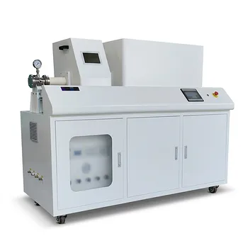
- Inclined Rotary Plasma Enhanced Chemical Vapor Deposition PECVD Equipment Tube Furnace Machine
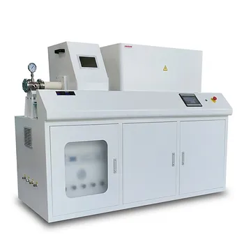
- Chemical Vapor Deposition CVD Equipment System Chamber Slide PECVD Tube Furnace with Liquid Gasifier PECVD Machine
- Inclined Rotary Plasma Enhanced Chemical Vapor Deposition PECVD Equipment Tube Furnace Machine
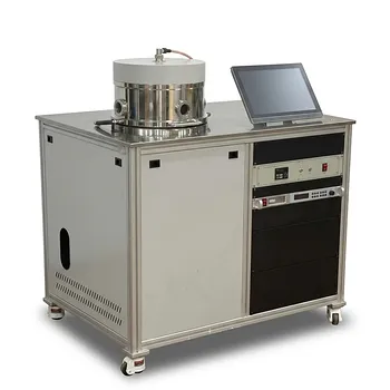
- RF PECVD System Radio Frequency Plasma-Enhanced Chemical Vapor Deposition RF PECVD
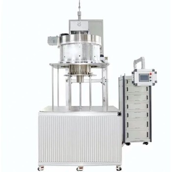
- Multi Heating Zones CVD Tube Furnace Machine Chemical Vapor Deposition Chamber System Equipment
People Also Ask
- What are the benefits of plasma enhanced CVD? Achieve High-Quality, Low-Temperature Film Deposition
- What is plasma enhanced chemical vapor deposition PECVD equipment? A Guide to Low-Temperature Thin Film Deposition
- How does PECVD facilitate Ru-C nanocomposite films? Precision Low-Temperature Thin Film Synthesis
- How does plasma enhanced chemical vapor deposition work? Enable Low-Temperature Thin Film Deposition
- What are the core advantages of PE-CVD in OLED encapsulation? Protect Sensitive Layers with Low-Temp Film Deposition
