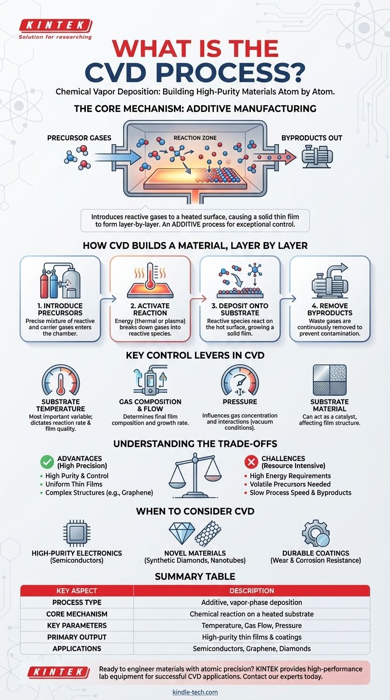
At its core, Chemical Vapor Deposition (CVD) is a sophisticated manufacturing process used to build high-purity, solid materials from the atom up. It works by introducing reactive gases into a chamber where they undergo a chemical reaction on or near a heated surface, known as a substrate. This reaction causes a thin film of solid material to form and deposit directly onto that substrate, creating everything from advanced semiconductor components to synthetic diamonds.
While many manufacturing methods involve shaping or subtracting from a solid block of material, CVD is fundamentally an additive process. It constructs a material layer-by-layer from a chemical vapor, offering exceptional control over purity, structure, and thickness.
How CVD Builds a Material, Layer by Layer
The CVD process can be understood as a highly controlled, four-step sequence. Each step is critical for ensuring the final material has the desired properties.
Step 1: Introducing the Precursors
The process begins by feeding a precise mixture of gases into a reaction chamber. These include precursor gases, which contain the necessary atoms for the final film (e.g., carbon-bearing gases for graphene), and often a carrier gas to dilute the reactants and control their flow.
Step 2: Activating the Reaction
For a reaction to occur, energy must be introduced. Most commonly, the substrate is heated to a very high temperature (often 800°C or higher). This thermal energy breaks down the precursor gases into highly reactive molecules, atoms, or radicals. In some variations, an RF plasma is used to achieve this activation at lower temperatures.
Step 3: Deposition onto the Substrate
The reactive gas species diffuse through the chamber and make contact with the substrate's surface. A chemical reaction takes place on this hot surface, causing the solid material to deposit and form a film. The substrate is not just a passive surface; it can act as a catalyst, initiating and guiding the chemical reaction to ensure the film adheres strongly and grows with the correct crystal structure.
Step 4: Removing the Byproducts
The chemical reactions that form the solid film also create unwanted gaseous byproducts. These waste gases are continuously removed from the chamber by a vacuum system. This final step is crucial for preventing contamination and maintaining the purity of the growing film.
The Key Control Levers in CVD
The quality, thickness, and structure of the final material are not accidental. They are the direct result of carefully managing several key process parameters.
Substrate Temperature
Temperature is arguably the single most important variable. It directly dictates the rate and type of chemical reactions that occur on the substrate surface. The wrong temperature can lead to poor film quality, impurities, or no deposition at all.
Gas Composition and Flow Rate
The specific mixture of precursor and carrier gases, along with the rate at which they are introduced into the chamber, determines the composition of the final film and its growth rate. Precise control over gas flow is essential for creating complex, multi-layered materials.
Pressure
The pressure inside the reaction chamber influences the concentration of gas molecules and how they interact. CVD is typically performed under carefully controlled vacuum conditions to ensure the purity and uniformity of the deposition process.
The Substrate Itself
The choice of substrate material is critical. In some applications, it is simply the object to be coated. In others, like the growth of graphene on copper foil, the substrate acts as a necessary catalyst for the entire reaction and determines the initial structure of the film.
Understanding the Trade-offs of CVD
While powerful, CVD is not a universal solution. Understanding its limitations is key to using it effectively.
High Energy Requirements
Most thermal CVD processes require extremely high temperatures to activate the necessary chemical reactions. This translates to significant energy consumption and requires equipment capable of safely operating under these conditions.
The Need for Volatile Precursors
CVD is dependent on having a gaseous source for the desired material. This means that a stable, volatile chemical precursor must exist for the elements you wish to deposit, which is not always possible or practical.
Process Speed and Byproduct Management
CVD can be a slow process, sometimes taking days or weeks to grow a thick, high-quality material like a synthetic diamond. Furthermore, the process can generate unwanted solid byproducts (like graphite forming alongside diamond) that may require the process to be stopped for cleaning.
When to Consider CVD for Your Project
Choosing a manufacturing process depends entirely on your end goal. CVD excels in specific applications where its unique capabilities provide a distinct advantage.
- If your primary focus is high-purity thin films for electronics: CVD offers unparalleled control over film composition, thickness, and uniformity, making it a cornerstone of the semiconductor industry.
- If your primary focus is creating novel or advanced materials: For materials like graphene, carbon nanotubes, or synthetic diamonds, CVD is a leading method because it can build precise crystalline structures from the ground up.
- If your primary focus is applying highly durable or functional coatings: CVD can produce thick, dense, and strongly adherent layers that provide exceptional wear resistance, corrosion protection, or thermal barriers.
Ultimately, Chemical Vapor Deposition is a foundational technology that empowers us to engineer materials with precision at the atomic scale.
Summary Table:
| Key Aspect | Description |
|---|---|
| Process Type | Additive, vapor-phase deposition |
| Core Mechanism | Chemical reaction of gases on a heated substrate |
| Key Parameters | Substrate temperature, gas composition, pressure |
| Primary Output | High-purity, high-performance thin films and coatings |
| Common Applications | Semiconductors, graphene, synthetic diamonds, wear-resistant coatings |
Ready to engineer materials with atomic precision? The CVD process is a cornerstone of advanced manufacturing, enabling the creation of high-purity thin films, semiconductors, and novel materials like graphene. KINTEK specializes in providing the high-performance lab equipment and consumables necessary to control the critical parameters of temperature, gas flow, and pressure for successful CVD applications. Let our experts help you select the right equipment to achieve unparalleled purity and performance in your materials. Contact our team today to discuss your specific laboratory needs and project goals.
Visual Guide
Related Products
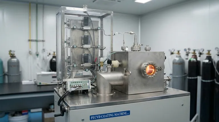
- Chemical Vapor Deposition CVD Equipment System Chamber Slide PECVD Tube Furnace with Liquid Gasifier PECVD Machine
- Customer Made Versatile CVD Tube Furnace Chemical Vapor Deposition Chamber System Equipment
- HFCVD Machine System Equipment for Drawing Die Nano-Diamond Coating
- Split Chamber CVD Tube Furnace with Vacuum Station Chemical Vapor Deposition System Equipment Machine
- Multi Heating Zones CVD Tube Furnace Machine Chemical Vapor Deposition Chamber System Equipment
People Also Ask
- What is the chemical vapor deposition growth process? Build Superior Thin Films from the Atom Up
- How expensive is chemical vapor deposition? Understanding the True Cost of High-Performance Coating
- How are carbon nanotubes grown? Master Scalable Production with Chemical Vapor Deposition
- What are the advantages of chemical vapor deposition? Achieve Superior Thin Films for Your Lab
- Why is Chemical Vapor Deposition (CVD) equipment uniquely suited for constructing hierarchical superhydrophobic structures?


