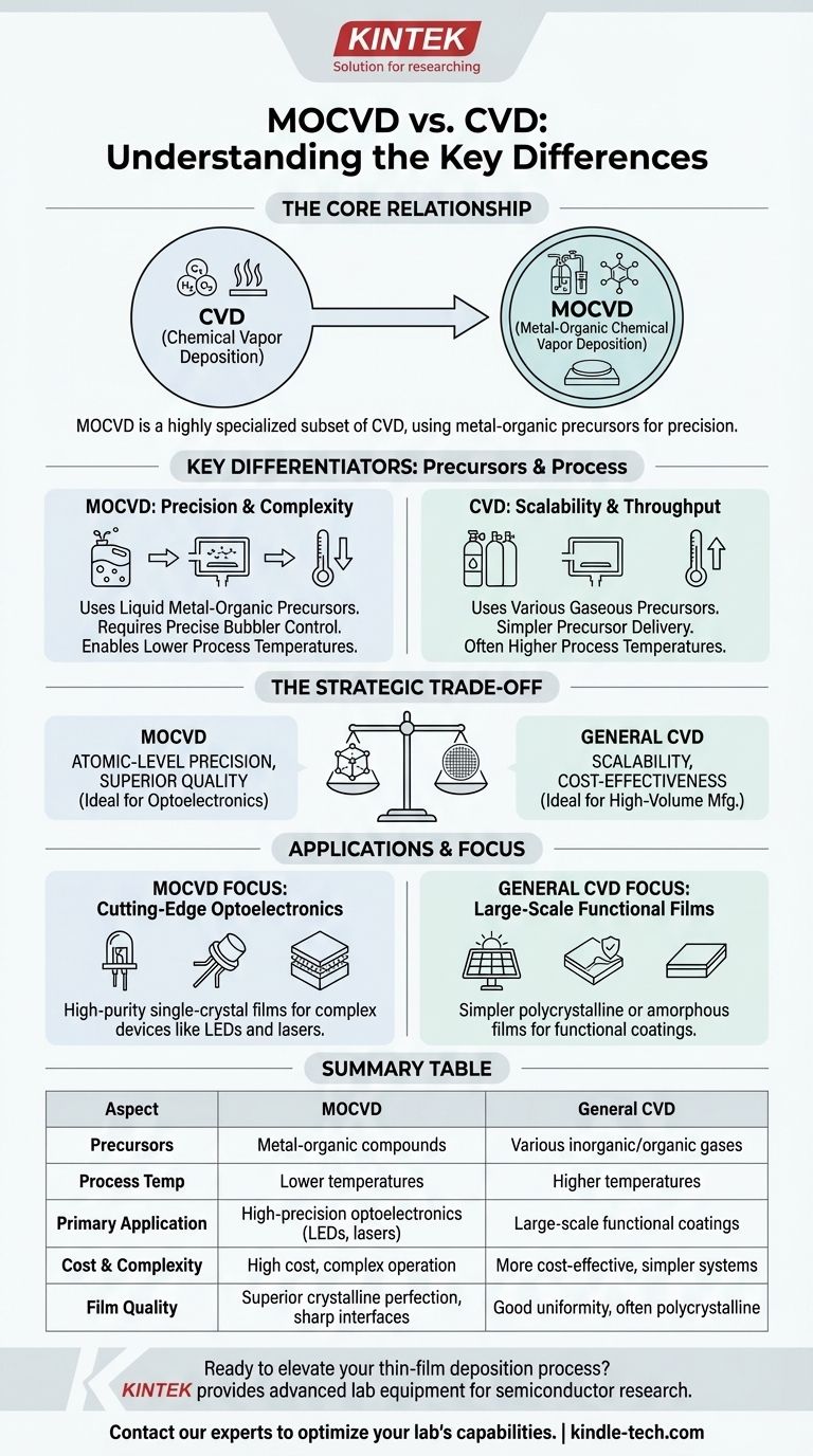
At its core, Metal-Organic Chemical Vapor Deposition (MOCVD) is not a rival to Chemical Vapor Deposition (CVD), but rather a highly specialized and advanced subset of it. The primary difference is MOCVD's use of metal-organic precursors, which enables lower process temperatures and exceptionally precise control over the growth of crystalline thin films, a capability essential for manufacturing advanced semiconductor devices.
The choice between MOCVD and other CVD methods is a strategic trade-off. It forces a decision between the atomic-level precision and superior quality offered by MOCVD versus the scalability and cost-effectiveness of more conventional CVD processes.
The Fundamental Divide: Precursors and Process Control
CVD is a broad category of processes used to deposit solid thin films from a gaseous state. MOCVD is one specific technique within this family, distinguished by a few key characteristics.
The Defining Difference: Precursor Materials
Chemical Vapor Deposition is defined by its use of chemical precursors that react and decompose on a substrate surface to create the desired film. The "type" of CVD is determined by the specific precursors used.
MOCVD is uniquely defined by its use of metal-organic precursors. These are complex compounds where a central metal atom is bonded to organic molecules. These precursors are often liquid at room temperature and must be carefully vaporized, typically using a "bubbler" system that flows a carrier gas through the liquid to transport the vapor to the reaction chamber.
Temperature and Complexity
MOCVD processes generally operate at lower temperatures compared to many other forms of CVD that deposit similar materials. This is a critical advantage for fabricating delicate crystalline structures, particularly in compound semiconductors like Gallium Arsenide (GaAs) or Gallium Nitride (GaN).
However, managing liquid metal-organic precursors introduces significant complexity. Achieving a reproducible and uniform film requires extremely precise control over bubbler temperature, gas flow rates, and chamber pressure. This makes MOCVD systems inherently more complex and expensive to operate.
Practical Implications: Precision vs. Scale
The technical differences between MOCVD and other CVD methods lead to very different ideal applications. The decision hinges on whether the goal is ultimate quality or industrial volume.
When to Use MOCVD: The Pursuit of Perfection
MOCVD is the tool of choice when atomic-level control is non-negotiable. Its primary advantage is the ability to grow high-purity, single-crystal thin films with exceptionally sharp interfaces between layers.
This precision is vital for creating complex heterostructures, where different materials are layered on top of each other with atomic accuracy. This makes MOCVD indispensable for fabricating high-performance optoelectronic devices like LEDs, laser diodes, and high-frequency transistors.
When to Use General CVD: The Need for Throughput
Broader CVD methods (like Atmospheric Pressure CVD or Low-Pressure CVD) are workhorses for applications where cost-effectiveness and high-volume manufacturing are the main drivers.
These processes are ideal for depositing simpler, often polycrystalline or amorphous films, such as silicon dioxide for insulation or silicon nitride for passivation layers. While they offer high purity and uniformity, they typically cannot match the crystalline perfection or abrupt interfaces achievable with MOCVD.
Understanding the Trade-offs
Choosing a deposition technology requires an objective look at its costs and limitations. MOCVD's precision comes with clear trade-offs.
Cost and Complexity
The sophisticated equipment needed for precise precursor delivery and process control makes MOCVD systems significantly more expensive than most conventional CVD setups. The metal-organic precursors themselves are also costly and can be toxic or pyrophoric, requiring specialized handling and safety infrastructure.
Application Limitations
While MOCVD excels at creating high-quality crystalline films for optoelectronics, it is not the universal solution. The references note it may not be the ideal choice for fabricating certain high-performance, power-hungry devices, where other deposition methods or materials might be better suited.
The CVD Family
It is crucial to remember that "CVD" is a family of techniques. Others include Plasma-Enhanced CVD (PECVD), which uses plasma to drive reactions at even lower temperatures, and Atomic Layer Deposition (ALD), which offers similar atomic-scale control but through a different, self-limiting process. MOCVD is simply one of the most advanced and precise members of this extensive family.
Making the Right Choice for Your Application
Your specific goal determines which deposition strategy is appropriate.
- If your primary focus is fabricating cutting-edge optoelectronics (LEDs, lasers): MOCVD is the industry standard, providing the necessary control to grow complex, high-quality crystalline heterostructures.
- If your primary focus is large-scale production of functional films (e.g., insulators, protective coatings): A more conventional and scalable CVD method will deliver the required throughput at a much lower cost per wafer.
- If your primary focus is advanced materials research with a flexible budget: MOCVD offers unparalleled control over film composition and structure, but its high cost and complexity must be justified by the need for its specific capabilities.
Ultimately, understanding this distinction empowers you to select the right tool for the job, transforming a material deposition challenge into a controlled, predictable manufacturing process.
Summary Table:
| Aspect | MOCVD | General CVD |
|---|---|---|
| Precursors | Metal-organic compounds | Various inorganic/organic gases |
| Process Temperature | Lower temperatures | Higher temperatures |
| Primary Application | High-precision optoelectronics (LEDs, lasers) | Large-scale functional coatings |
| Cost & Complexity | High cost, complex operation | More cost-effective, simpler systems |
| Film Quality | Superior crystalline perfection, sharp interfaces | Good uniformity, often polycrystalline |
Ready to elevate your thin-film deposition process? KINTEK specializes in providing advanced lab equipment and consumables for semiconductor research and manufacturing. Whether you're developing next-generation optoelectronics with MOCVD or scaling up production with CVD, our expertise ensures you have the right tools for precise, reliable results. Contact our experts today to discuss how our solutions can optimize your laboratory's capabilities and drive your innovations forward.
Visual Guide
Related Products
- Multi Heating Zones CVD Tube Furnace Machine Chemical Vapor Deposition Chamber System Equipment
- 915MHz MPCVD Diamond Machine Microwave Plasma Chemical Vapor Deposition System Reactor
- Microwave Plasma Chemical Vapor Deposition MPCVD Machine System Reactor for Lab and Diamond Growth
- Cylindrical Resonator MPCVD Machine System Reactor for Microwave Plasma Chemical Vapor Deposition and Lab Diamond Growth
- Molybdenum Vacuum Heat Treat Furnace
People Also Ask
- What advantages do CVD furnaces offer for Wf/W composites? Preserving Fiber Ductility and Interface Integrity
- What is a CVD tube furnace? A Complete Guide to Thin-Film Deposition
- What are the differences between chemical vapour deposition processes? A Guide to Pressure, Quality & Cost
- What are the advantages of using a Multi-zone Tube Furnace? Enhanced Thermal Uniformity for Diffusion Research
- What is the function of a high-temperature CVD tube furnace in 3D graphene foam prep? Master 3D Nanomaterial Growth