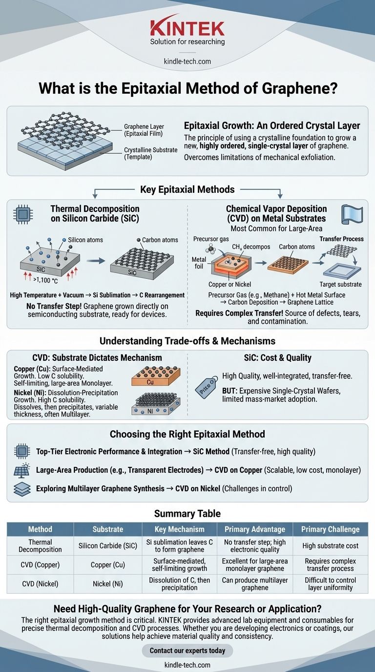
Epitaxial growth of graphene refers to a category of methods where a thin, highly ordered, single-crystal layer of graphene is grown on the surface of a crystalline substrate. The two primary techniques are the thermal decomposition of silicon carbide (SiC) and Chemical Vapor Deposition (CVD) on catalytic metal substrates. In both cases, the underlying crystal structure of the substrate acts as a template, guiding the carbon atoms to form a high-quality graphene lattice.
Epitaxy is not a single method but a principle: using a crystalline foundation to grow a new, ordered crystal layer on top. For graphene, this approach is used to create large-area, high-quality films, a significant advantage over the small, randomly-oriented flakes produced by methods like mechanical exfoliation.
The Principle of Epitaxy: Growing an Ordered Crystal
What "Epitaxy" Means
The term epitaxy originates from the Greek roots epi ("above") and taxis ("in ordered manner"). It describes the deposition of a crystalline overlayer on a crystalline substrate.
Think of the substrate as a perfectly laid tile foundation. Epitaxial growth is like carefully placing new tiles (the graphene atoms) so that they align perfectly with the pattern of the foundation below, creating a large, seamless new floor.
Why Use Epitaxy for Graphene?
While mechanical exfoliation (the "Scotch tape method") can produce pristine graphene flakes, the process yields small, randomly placed samples. This is excellent for lab research but impractical for industrial-scale electronics or coatings.
Epitaxial methods are designed to overcome this limitation. They aim to produce wafer-scale, continuous films of graphene with consistent quality, making them suitable for integration into manufacturing processes.
Key Epitaxial Methods for Graphene
Thermal Decomposition on Silicon Carbide (SiC)
This method involves heating a single-crystal SiC wafer to very high temperatures (above 1,100 °C) in a high vacuum.
At these temperatures, silicon atoms sublimate (turn from solid to gas) away from the surface faster than the carbon atoms. The remaining carbon atoms on the surface spontaneously rearrange to form one or more layers of graphene.
A key advantage here is that the graphene is grown directly on a semiconducting or insulating substrate, making it immediately ready for fabricating electronic devices without a transfer step.
Chemical Vapor Deposition (CVD) on Metal Substrates
CVD is the most common method for large-area graphene synthesis. A polished metal foil, typically copper (Cu) or nickel (Ni), is placed in a furnace.
A carbon-containing precursor gas, like methane (CH₄), is introduced into the chamber. At high temperatures (around 1,000 °C), the precursor gas decomposes, and carbon atoms deposit onto the hot metal surface, where they assemble into a graphene lattice.
After growth, the graphene film must be transferred from the metal foil to a target substrate (like glass or silicon) for most applications.
Understanding the Trade-offs and Mechanisms
The Substrate Dictates the Mechanism
The choice of metal substrate in CVD fundamentally changes the growth process.
Surface-Mediated Growth (Copper): Copper has very low carbon solubility. Graphene growth occurs exclusively on the surface, and the process is largely self-limiting once a full monolayer covers the copper. This makes it the preferred method for producing high-quality, large-area monolayer graphene.
Dissolution-Precipitation Growth (Nickel): Nickel has a much higher solubility for carbon. At growth temperatures, carbon atoms dissolve into the bulk of the nickel. As the metal cools, the carbon's solubility decreases, causing it to precipitate back to the surface, forming graphene. This process can be difficult to control and often results in multilayer graphene with variable thickness.
The Transfer Challenge with CVD
The biggest drawback of the CVD method is the necessity of a transfer process. The graphene layer must be coated with a polymer support, the metal etched away, and the remaining polymer/graphene film transferred to a new substrate.
This complex process is a major source of defects, tears, wrinkles, and contamination, which can degrade the exceptional electronic properties of the pristine graphene.
The Cost and Quality of SiC
Epitaxial growth on SiC avoids the damaging transfer step, resulting in very high-quality graphene that is well-integrated with its substrate.
However, single-crystal SiC wafers are significantly more expensive than the metal foils used in CVD, which has limited its adoption for mass-market applications. The interaction between the graphene and the SiC substrate can also subtly alter the graphene's electronic properties.
Choosing the Right Epitaxial Method
To select the appropriate technique, you must first define your primary goal. The "best" method depends entirely on your specific application and constraints.
- If your primary focus is top-tier electronic performance and device integration: The SiC method is often preferred for its transfer-free process and the high quality of the resulting graphene-on-substrate system.
- If your primary focus is large-area production for applications like transparent electrodes or composites: CVD on copper is the dominant industrial choice due to its scalability, lower cost, and ability to produce continuous monolayer films.
- If your primary focus is exploring the synthesis of multilayer graphene: CVD on nickel or other high-solubility metals provides a pathway, but be prepared for significant challenges in controlling layer uniformity and thickness.
Understanding these core principles allows you to select the epitaxial technique that best aligns with your specific material quality and application requirements.
Summary Table:
| Method | Substrate | Key Mechanism | Primary Advantage | Primary Challenge |
|---|---|---|---|---|
| Thermal Decomposition | Silicon Carbide (SiC) | Silicon sublimation leaves carbon to form graphene | No transfer step; high electronic quality | High substrate cost |
| CVD (Copper) | Copper (Cu) | Surface-mediated, self-limiting growth | Excellent for large-area monolayer graphene | Requires complex transfer process |
| CVD (Nickel) | Nickel (Ni) | Dissolution of carbon, then precipitation | Can produce multilayer graphene | Difficult to control layer uniformity |
Need High-Quality Graphene for Your Research or Application?
The right epitaxial growth method is critical for your project's success. KINTEK specializes in providing the advanced lab equipment and consumables needed for precise thermal decomposition and CVD processes. Whether you are developing next-generation electronics or large-area coatings, our solutions help you achieve the material quality and consistency you require.
Contact our experts today to discuss how we can support your graphene synthesis and integration challenges.
Visual Guide
Related Products
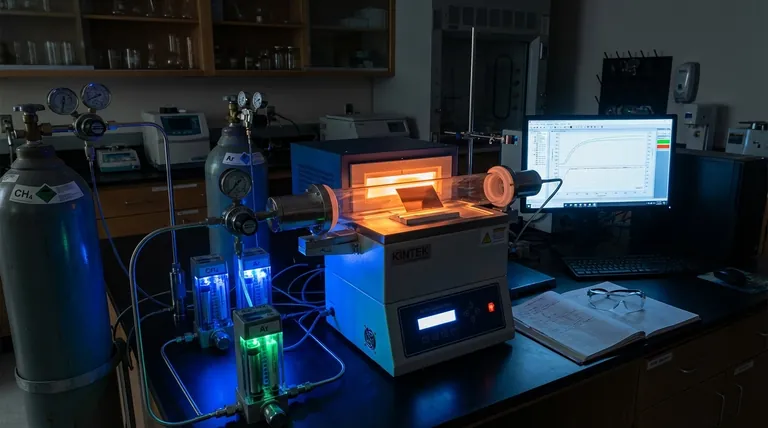
- Customer Made Versatile CVD Tube Furnace Chemical Vapor Deposition Chamber System Equipment
- Chemical Vapor Deposition CVD Equipment System Chamber Slide PECVD Tube Furnace with Liquid Gasifier PECVD Machine
- HFCVD Machine System Equipment for Drawing Die Nano-Diamond Coating
- RF PECVD System Radio Frequency Plasma-Enhanced Chemical Vapor Deposition RF PECVD
- Multi Heating Zones CVD Tube Furnace Machine Chemical Vapor Deposition Chamber System Equipment
People Also Ask
- How is graphene synthesized? Choosing the Right Method for Your Application
- What is the application of CVD in nanotechnology? Harness Atomic-Level Precision for Next-Gen Materials
- What method is used to grow graphene? Master High-Quality Production with CVD
- What is the function of a high-temperature CVD tube furnace in 3D graphene foam prep? Master 3D Nanomaterial Growth
- What is the difference between hot wall CVD and cold wall CVD? Choose the Right System for Your Process


