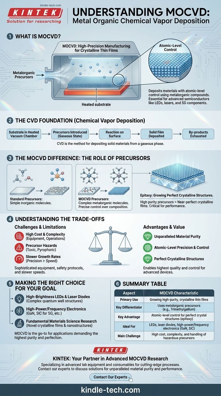
At its core, Metal Organic Chemical Vapor Deposition (MOCVD) is a highly precise manufacturing process used to grow high-purity crystalline thin films. It is a specific type of Chemical Vapor Deposition (CVD) distinguished by its use of metalorganic compounds as the chemical precursors. These precursors are delivered as a vapor into a reaction chamber to deposit materials with atomic-level control, making it essential for producing advanced semiconductors.
MOCVD is not just a coating technique; it's a method for constructing materials from the ground up. By carefully controlling the flow of specific metal-containing gases over a heated surface, it enables the creation of perfect crystalline layers that form the foundation of high-performance electronics like LEDs, lasers, and 5G components.
How Chemical Vapor Deposition (CVD) Works
To understand MOCVD, we must first understand the fundamental process of Chemical Vapor Deposition (CVD) it is built upon. CVD is a method for depositing solid materials from a gaseous phase.
The Basic Setup
The process begins by placing a substrate—the material to be coated—inside a reaction chamber. This chamber is typically heated and kept under a controlled vacuum.
Introducing the Precursors
One or more volatile chemical compounds, known as precursors, are introduced into the chamber in a gaseous state. These precursors contain the elements required to form the desired thin film.
The Deposition Reaction
When the precursor gases flow over the hot substrate, they undergo a chemical reaction or decomposition. This reaction causes the desired solid material to "deposit" or bond onto the substrate's surface.
Building the Thin Film
This deposition occurs across the entire exposed surface of the substrate, gradually building up a uniform, solid thin film. Any volatile by-products from the reaction are exhausted from the chamber by a continuous gas flow. This general process is used to create everything from wear-resistant coatings on cutting tools to photovoltaic layers in solar cells.
The MOCVD Difference: The Critical Role of Precursors
While the general mechanics are similar to CVD, the power of MOCVD lies in its choice of precursors. This is what sets it apart and makes it indispensable for modern electronics.
What Are Metalorganic Precursors?
MOCVD uses metalorganic precursors. These are complex molecules where a central metal atom (like Gallium, Aluminum, or Indium) is chemically bonded to organic molecules.
For example, Trimethylgallium (TMGa) is a common precursor that provides the Gallium needed to create Gallium Nitride (GaN) films.
The Advantage of Control
Metalorganic precursors are liquids or solids that are highly volatile, meaning they can be easily vaporized and transported into the reaction chamber with extreme precision. This allows engineers to control the chemical composition of the growing film with atomic-level accuracy.
By precisely mixing different precursor gases, it's possible to create complex compound semiconductors and alloys. This process of growing a perfect, single-crystal layer on top of a crystalline substrate is known as epitaxy.
The Result: Perfect Crystalline Structures
The high purity of metalorganic precursors and the precise control of the MOCVD process allow for the growth of near-perfect crystalline films. This structural perfection is absolutely critical for the performance of electronic and optoelectronic devices, where even minor defects can degrade or destroy function.
Understanding the Trade-offs
MOCVD is a powerful technique, but its precision comes with inherent challenges and limitations that are important to understand.
High Cost and Complexity
MOCVD reactors are sophisticated, complex systems that represent a significant capital investment. The operational costs are also high due to the need for high-purity gases, vacuum systems, and precise temperature and pressure controls.
Precursor Hazards
The metalorganic precursors used in MOCVD are often highly toxic and pyrophoric, meaning they can spontaneously ignite upon contact with air. This necessitates stringent safety protocols, specialized handling equipment, and robust facility design, adding to the overall complexity and cost.
Precision Over Speed
MOCVD is designed for exceptional quality and control, not high-speed bulk deposition. The growth rates are relatively slow compared to other methods, making it best suited for creating the thin, critical active layers of a device rather than depositing thick, structural coatings.
Making the Right Choice for Your Goal
MOCVD is the go-to process for applications demanding the highest level of material purity and structural perfection.
- If your primary focus is manufacturing high-brightness LEDs and laser diodes: MOCVD is the industry-standard technology for creating the complex quantum well structures that emit light efficiently.
- If your primary focus is developing high-power or high-frequency electronics: MOCVD is essential for growing the Gallium Nitride (GaN) and Silicon Carbide (SiC) films that vastly outperform traditional silicon in these applications.
- If your primary focus is fundamental materials science research: MOCVD provides an unparalleled platform for exploring and synthesizing novel crystalline thin films and nanostructures with precise control over their properties.
Ultimately, MOCVD is the enabling technology behind many of the devices that define our modern world, from the screen you are reading to the networks that connect us.
Summary Table:
| Aspect | MOCVD Characteristic |
|---|---|
| Primary Use | Growing high-purity, crystalline thin films |
| Key Differentiator | Uses metalorganic precursors (e.g., Trimethylgallium) |
| Key Advantage | Atomic-level control for perfect crystal structures (epitaxy) |
| Ideal For | LEDs, laser diodes, high-power/frequency electronics (GaN, SiC) |
| Main Challenge | High cost, complexity, and handling of hazardous precursors |
Ready to advance your semiconductor or optoelectronic research with precision thin films?
KINTEK specializes in providing the advanced lab equipment and consumables needed for cutting-edge MOCVD processes. Our expertise supports laboratories in developing next-generation devices, from high-efficiency LEDs to powerful 5G components.
Contact our experts today via our secure form to discuss how our solutions can help you achieve unparalleled material purity and performance in your projects.
Visual Guide
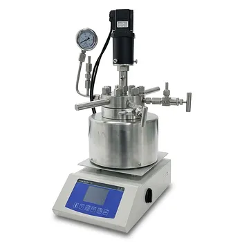
Related Products
- 915MHz MPCVD Diamond Machine Microwave Plasma Chemical Vapor Deposition System Reactor
- Cylindrical Resonator MPCVD Machine System Reactor for Microwave Plasma Chemical Vapor Deposition and Lab Diamond Growth
- Microwave Plasma Chemical Vapor Deposition MPCVD Machine System Reactor for Lab and Diamond Growth
- Customer Made Versatile CVD Tube Furnace Chemical Vapor Deposition Chamber System Equipment
- Multi Heating Zones CVD Tube Furnace Machine Chemical Vapor Deposition Chamber System Equipment
People Also Ask
- What is microwave plasma CVD? A Guide to High-Purity Diamond and Material Synthesis
- How do vacuum pumps and valves collaborate in MPCVD? Achieve Precise Pressure Control for Superior CNT Synthesis
- How are CVD diamonds created? Discover the Science of Lab-Grown Diamond Precision
- What pressure is needed for chemical vapor deposition of diamonds? Master the Low-Pressure 'Sweet Spot'
- Why is MW-CVD preferred for high-purity diamond optical windows? Achieve Zero-Contamination Material Growth