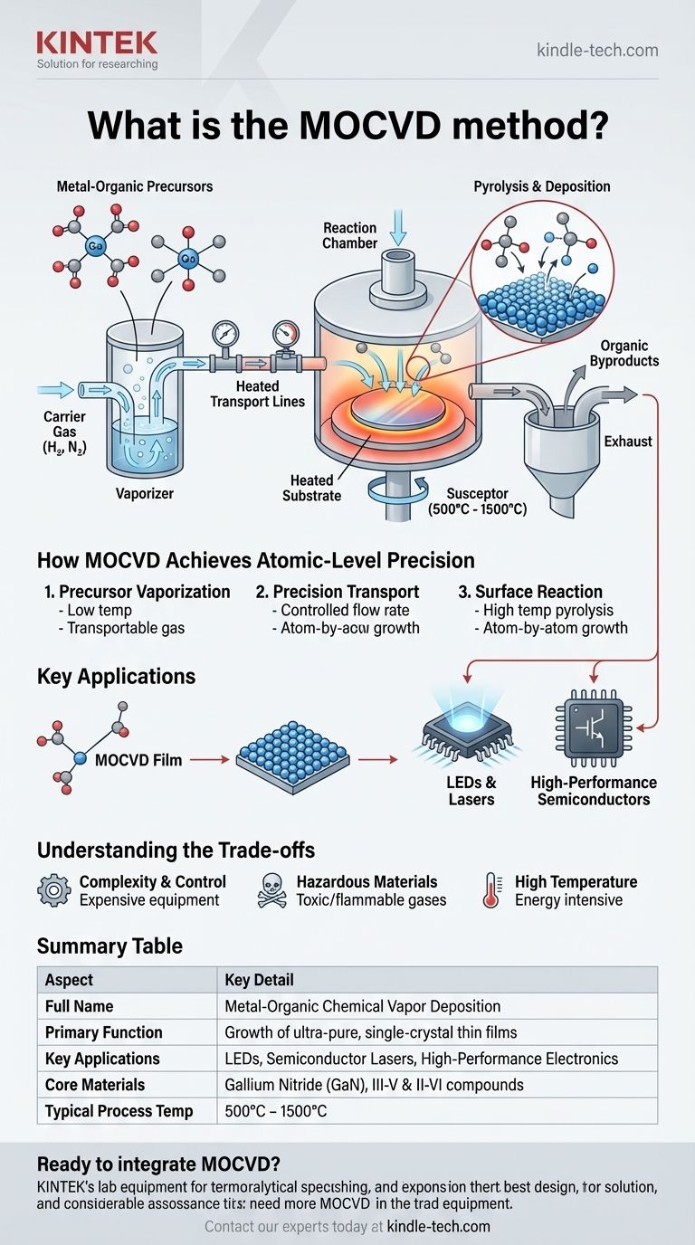
At its core, Metal-Organic Chemical Vapor Deposition (MOCVD) is a highly controlled chemical process used to grow ultra-pure, single-crystal thin films onto a substrate. It functions by introducing volatile metal-organic compounds in a gas stream into a reaction chamber, where they decompose on a heated wafer. This decomposition reaction deposits material atom-by-atom, forming the perfect crystalline structures essential for manufacturing high-performance electronic and photonic devices like LEDs and lasers.
To manufacture the advanced semiconductors that power our world, you must be able to create flawless, wafer-thin layers of crystalline material. MOCVD achieves this through precisely controlled surface chemistry, making it a scalable and dominant method for producing the foundational materials of modern high-performance electronics.
How MOCVD Achieves Atomic-Level Precision
MOCVD is a sophisticated process that relies on the interplay of chemistry, thermodynamics, and fluid dynamics. Each stage is engineered for maximum control over the final material's properties.
The Role of Metal-Organic Precursors
The process begins with metal-organic (MO) precursors, which are specialized chemical compounds. These molecules contain the desired metal atom (such as gallium, indium, or zinc) attached to volatile organic groups.
This structure gives them a key property: they can be easily vaporized at low temperatures, allowing them to be transported as a gas.
The Vapor Phase Transport System
A carrier gas, such as hydrogen or nitrogen, is bubbled through the liquid MO precursor. This process, known as vaporization, picks up a precise concentration of the precursor molecules.
This gas mixture is then transported through a series of pipes and valves, which precisely control the flow rate, into the main reaction chamber.
Chemical Reaction on the Heated Substrate
Inside the chamber, a substrate (typically a silicon or sapphire wafer) is heated to very high temperatures, often between 500°C and 1500°C.
When the precursor gases hit this hot surface, they undergo a chemical reaction called pyrolysis. The heat breaks the chemical bonds, causing the metal atoms to deposit onto the substrate surface, where they self-assemble into a perfect crystalline lattice. The leftover organic byproducts are simply swept out of the chamber by the gas flow.
Key Applications in Modern Technology
MOCVD's ability to produce high-quality, uniform films makes it indispensable for several high-tech industries.
Manufacturing LEDs and Lasers
MOCVD is the dominant technology for manufacturing high-brightness LEDs and semiconductor lasers, especially those based on gallium nitride (GaN).
Its precise control over layering different materials is critical for creating the structures that emit light efficiently.
Building High-Performance Semiconductors
The method is also used to create high-power and high-speed electronic devices. The purity and crystalline perfection of MOCVD-grown films are essential for transistors and integrated circuits that operate under demanding conditions.
Understanding the Trade-offs of MOCVD
While powerful, MOCVD is not without its complexities and challenges. Understanding these trade-offs is key to appreciating its role.
Complexity and Process Control
The primary advantage of MOCVD—its precision—is also a source of complexity. The system requires meticulous control over gas flows, pressure, and temperature to ensure repeatable, high-quality results. This makes the equipment sophisticated and expensive.
Use of Hazardous Materials
The metal-organic precursors and carrier gases are often highly toxic and flammable. Consequently, MOCVD systems require robust safety protocols, leak detection systems, and tail gas treatment facilities to neutralize harmful exhaust byproducts.
High Temperature Requirements
The high growth temperatures consume significant energy and can limit the types of substrate materials that can be used. Materials that cannot withstand such heat are incompatible with the standard MOCVD process.
Making the Right Choice for Your Goal
Deciding whether to use MOCVD depends entirely on the material requirements and production goals of your project.
- If your primary focus is mass-producing high-brightness LEDs or laser diodes: MOCVD is the industry standard due to its scalability and unmatched ability to produce high-quality GaN-based films.
- If your primary focus is creating complex, multi-layer semiconductor devices: MOCVD offers excellent control over film composition, thickness, and doping, making it a powerful tool for both research and production.
- If your primary focus is working with temperature-sensitive substrates or requiring ultimate film purity for fundamental research: You may need to evaluate alternatives like Molecular Beam Epitaxy (MBE), which operates at lower temperatures in an ultra-high vacuum environment.
Ultimately, understanding MOCVD is to understand the chemical foundation upon which much of our modern electronic and photonic world is built.
Summary Table:
| Aspect | Key Detail |
|---|---|
| Full Name | Metal-Organic Chemical Vapor Deposition |
| Primary Function | Growth of ultra-pure, single-crystal thin films |
| Key Applications | LEDs, Semiconductor Lasers, High-Performance Electronics |
| Core Materials | Gallium Nitride (GaN), other III-V & II-VI compounds |
| Typical Process Temperature | 500°C - 1500°C |
Ready to integrate MOCVD technology into your laboratory workflow? KINTEK specializes in providing the advanced lab equipment and consumables you need for cutting-edge materials development. Whether you are scaling up LED production or pushing the boundaries of semiconductor research, our expertise can help you achieve precise and reliable results. Contact our experts today to discuss how we can support your specific project goals with tailored solutions.
Visual Guide
Related Products
- Multi Heating Zones CVD Tube Furnace Machine Chemical Vapor Deposition Chamber System Equipment
- 915MHz MPCVD Diamond Machine Microwave Plasma Chemical Vapor Deposition System Reactor
- Microwave Plasma Chemical Vapor Deposition MPCVD Machine System Reactor for Lab and Diamond Growth
- Cylindrical Resonator MPCVD Machine System Reactor for Microwave Plasma Chemical Vapor Deposition and Lab Diamond Growth
- Molybdenum Vacuum Heat Treat Furnace
People Also Ask
- How does a CVD tube furnace inhibit the sintering of silver supports? Boost Membrane Durability and Performance
- What is a CVD tube furnace? A Complete Guide to Thin-Film Deposition
- What is the function of a tube furnace in CVD SiC synthesis? Achieving Ultra-Pure Silicon Carbide Powders
- What advantages do CVD furnaces offer for Wf/W composites? Preserving Fiber Ductility and Interface Integrity
- What are the differences between chemical vapour deposition processes? A Guide to Pressure, Quality & Cost